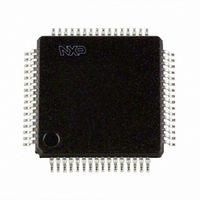
P89LPC9402FBD,557 NXP Semiconductors, P89LPC9402FBD,557 Datasheet - Page 40

P89LPC9402FBD,557
Manufacturer Part Number
P89LPC9402FBD,557
Description
IC 80C51 MCU FLASH 8K 64-LQFP
Manufacturer
NXP Semiconductors
Series
LPC900r
Datasheet
1.P89LPC9402FBD557.pdf
(60 pages)
Specifications of P89LPC9402FBD,557
Program Memory Type
FLASH
Program Memory Size
8KB (8K x 8)
Package / Case
64-LQFP
Core Processor
8051
Core Size
8-Bit
Speed
18MHz
Connectivity
I²C, SPI, UART/USART
Peripherals
Brown-out Detect/Reset, LCD, LED, POR, PWM, WDT
Number Of I /o
23
Ram Size
256 x 8
Voltage - Supply (vcc/vdd)
2.4 V ~ 3.6 V
Oscillator Type
Internal
Operating Temperature
-40°C ~ 85°C
Processor Series
P89LPC
Core
80C51
Data Bus Width
8 bit
Data Ram Size
256 B
Interface Type
I2C, SPI, UART
Maximum Clock Frequency
18 MHz
Number Of Programmable I/os
20
Number Of Timers
2
Operating Supply Voltage
2.4 V to 3.6 V
Maximum Operating Temperature
+ 85 C
Mounting Style
SMD/SMT
3rd Party Development Tools
PK51, CA51, A51, ULINK2
Minimum Operating Temperature
- 40 C
Lead Free Status / RoHS Status
Lead free / RoHS Compliant
Eeprom Size
-
Data Converters
-
Lead Free Status / Rohs Status
Lead free / RoHS Compliant
Other names
935288631557
Available stocks
Company
Part Number
Manufacturer
Quantity
Price
Company:
Part Number:
P89LPC9402FBD,557
Manufacturer:
NXP Semiconductors
Quantity:
10 000
NXP Semiconductors
P89LPC9402_1
Product data sheet
7.27.13.1 I
7.27.12 Input bank selector
7.27.13 Blinker
7.27.14 Input filters
7.27.15 I
The input bank selector loads display data into the display RAM based on the selected
LCD drive configuration. The BANK SELECT command can be used to load display data
in bit 2 in static drive mode or in bits 2 and 3 in 1:2 mode. The input bank selector
functions are independent of the output bank selector.
The LCD controller has a very versatile display blinking capability. The whole display can
blink at a frequency selected by the BLINK command. Each blink frequency is a multiple
integer value of the clock frequency; the ratio between the clock frequency and blink
frequency depends on the blink mode selected, as shown in
An additional feature allows an arbitrary selection of LCD segments to be blinked in the
static and 1:2 drive modes. This is implemented without any communication overheads by
the output bank selector which alternates the displayed data between the data in the
display RAM bank and the data in an alternative RAM bank at the blink frequency. This
mode can also be implemented by the BLINK command.
The entire display can be blinked at a frequency other than the nominal blink frequency by
sequentially resetting and setting the display enable bit E at the required rate using the
MODE SET command.
Table 9.
Blink modes 0.5 Hz, 1 Hz and 2 Hz, and nominal blink frequencies 0.5 Hz, 1 Hz and 2 Hz
correspond to an oscillator frequency (f
frequency range is 397 Hz to 3046 Hz.
The LCD controller acts as an I
subaddress inputs A0, A,1 and A2 are tied to V
To enhance noise immunity in electrically adverse environments, RC low-pass filters are
provided on the SDA and SCL lines.
The I
not respond to a read access.
Blink mode
Off
2 Hz
1 Hz
0.5 Hz
2
2
C-bus controller
C-bus slave addresses
2
C-bus slave address is 0111 0000. The LCD controller is a write-only device and will
Blinking frequencies
Rev. 01 — 22 April 2009
8-bit microcontroller with accelerated two-clock 80C51 core
Normal operating mode ratio Normal blink frequency
-
f
f
f
osc(LCD)
osc(LCD)
osc(LCD)
2
C-bus slave receiver. In the P89LPC9402 the hardware
/768
/1536
/3072
osc(LCD)
) of 1536 Hz at pin CLK. The oscillator
SS
setting the hardware subaddress = 0.
Blinking off
2 Hz
1 Hz
0.5 Hz
Table
P89LPC9402
9.
© NXP B.V. 2009. All rights reserved.
40 of 60


