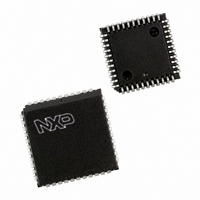
P89LV51RD2FA,512 NXP Semiconductors, P89LV51RD2FA,512 Datasheet - Page 7

P89LV51RD2FA,512
Manufacturer Part Number
P89LV51RD2FA,512
Description
IC 80C51 MCU 1024 RAM 44PLCC
Manufacturer
NXP Semiconductors
Series
89LVr
Datasheet
1.P89LV51RD2BBC557.pdf
(76 pages)
Specifications of P89LV51RD2FA,512
Core Processor
8051
Core Size
8-Bit
Speed
33MHz
Connectivity
SPI, UART/USART
Peripherals
Brown-out Detect/Reset, POR, PWM, WDT
Number Of I /o
32
Program Memory Size
64KB (64K x 8)
Program Memory Type
FLASH
Ram Size
1K x 8
Voltage - Supply (vcc/vdd)
2.7 V ~ 3.6 V
Oscillator Type
Internal
Operating Temperature
-40°C ~ 85°C
Package / Case
44-PLCC
Processor Series
P89LV5x
Core
80C51
Data Bus Width
8 bit
Data Ram Size
1 KB
Interface Type
SPI, UART
Maximum Clock Frequency
33 MHz
Number Of Programmable I/os
32
Number Of Timers
3
Operating Supply Voltage
2.4 V to 3.6 V
Maximum Operating Temperature
+ 85 C
Mounting Style
SMD/SMT
3rd Party Development Tools
PK51, CA51, A51, ULINK2
Minimum Operating Temperature
- 40 C
Package
44PLCC
Device Core
80C51
Family Name
89LV
Maximum Speed
40 MHz
For Use With
622-1017 - BOARD 44-ZIF PLCC SOCKET622-1008 - BOARD FOR LPC9103 10-HVSON
Lead Free Status / RoHS Status
Lead free / RoHS Compliant
Eeprom Size
-
Data Converters
-
Lead Free Status / Rohs Status
Details
Other names
935274176512
P89LV51RD2FA
P89LV51RD2FA
P89LV51RD2FA
P89LV51RD2FA
Available stocks
Company
Part Number
Manufacturer
Quantity
Price
Company:
Part Number:
P89LV51RD2FA,512
Manufacturer:
NXP Semiconductors
Quantity:
10 000
Part Number:
P89LV51RD2FA,512
Manufacturer:
NXP/恩智浦
Quantity:
20 000
NXP Semiconductors
Table 3.
P89LV51RB2_RC2_RD2_5
Product data sheet
Symbol
P1.3/CEX0
P1.4/SS/CEX1
P1.5/MOSI/
CEX2
P1.6/MISO/
CEX3
P1.7/SPICLK/
CEX4
P2.0 to P2.7
P2.0/A8
P2.1/A9
P2.2/A10
P2.3/A11
P2.4/A12
P2.5/A13
P2.6/A14
P89LV51RB2/RC2/RD2 pin description
Pin
TQFP44
43
44
1
2
3
18
19
20
21
22
23
24
PLCC44
5
6
7
8
9
24
25
26
27
28
29
30
Type
I/O
I/O
I/O
I
I/O
I/O
I/O
I/O
I/O
I/O
I/O
I/O
I/O
I/O
I/O with
internal
pull-up
I/O
O
I/O
O
I/O
O
I/O
O
I/O
O
I/O
O
I/O
O
Rev. 05 — 15 December 2009
…continued
Description
P1.3 — Port 1 bit 3.
CEX0 — Capture/compare external I/O for PCA Module 0. Each
capture/compare module connects to a Port 1 pin for external
I/O. When not used by the PCA, this pin can handle standard I/O.
P1.4 — Port 1 bit 4.
SS — Slave port select input for SPI.
CEX1 — Capture/compare external I/O for PCA Module 1.
P1.5 — Port 1 bit 5.
MOSI — Master Output Slave Input for SPI.
CEX2 — Capture/compare external I/O for PCA Module 2.
P1.6 — Port 1 bit 6.
MISO — Master Input Slave Output for SPI.
CEX3 — Capture/compare external I/O for PCA Module 3.
P1.7 — Port 1 bit 7.
SPICLK — Serial clock input/output for SPI.
CEX4 — Capture/compare external I/O for PCA Module 4.
Port 2: Port 2 is an 8-bit bidirectional I/O port with internal
pull-ups. Port 2 pins are pulled HIGH by the internal pull-ups
when ‘1’s are written to them and can be used as inputs in this
state. As inputs, Port 2 pins that are externally pulled LOW will
source current (I
the high-order address byte during fetches from external
program memory and during accesses to external Data Memory
that use 16-bit address (MOVX@DPTR). In this application, it
uses strong internal pull-ups when transitioning to ‘1’s. Port 2
also receives some control signals and a partial of high-order
address bits during the external host mode programming and
verification.
P2.0 — Port 2 bit 0.
A8 — Address bit 8.
P2.1 — Port 2 bit 1.
A9 — Address bit 9.
P2.2 — Port 2 bit 2.
A10 — Address bit 10.
P2.3 — Port 2 bit 3.
A11 — Address bit 11.
P2.4 — Port 2 bit 4.
A12 — Address bit 12.
P2.5 — Port 2 bit 5.
A13 — Address bit 13.
P2.6 — Port 2 bit 6.
A14 — Address bit 14.
P89LV51RB2/RC2/RD2
IL
) because of the internal pull-ups. Port 2 sends
8-bit microcontrollers with 80C51 core
© NXP B.V. 2009. All rights reserved.
7 of 76


