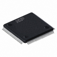
LPC2923FBD100,551 NXP Semiconductors, LPC2923FBD100,551 Datasheet - Page 12

LPC2923FBD100,551
Manufacturer Part Number
LPC2923FBD100,551
Description
IC ARM9 MCU FLASH 256KB 100-LQFP
Manufacturer
NXP Semiconductors
Series
LPC2900r
Datasheet
1.LPC2921FBD100551.pdf
(84 pages)
Specifications of LPC2923FBD100,551
Core Processor
ARM9
Core Size
32-Bit
Speed
125MHz
Connectivity
CAN, I²C, LIN, SPI, UART/USART, USB
Peripherals
DMA, POR, PWM, WDT
Number Of I /o
60
Program Memory Size
256KB (256K x 8)
Program Memory Type
FLASH
Eeprom Size
16K x 8
Ram Size
24K x 8
Voltage - Supply (vcc/vdd)
1.71 V ~ 3.6 V
Data Converters
A/D 16x8b
Oscillator Type
Internal
Operating Temperature
-40°C ~ 85°C
Package / Case
100-LQFP
Processor Series
LPC29
Core
ARM968E-S
3rd Party Development Tools
MDK-ARM, RL-ARM, ULINK2
Lead Free Status / RoHS Status
Lead free / RoHS Compliant
Other names
935287115551
Available stocks
Company
Part Number
Manufacturer
Quantity
Price
Company:
Part Number:
LPC2923FBD100,551
Manufacturer:
NXP Semiconductors
Quantity:
10 000
NXP Semiconductors
1.
LPC2921_23_25_3
Product data sheet
Only for 1.8 V power sources
6.6.1 Reset and power-up behavior
6.6.2 Reset strategy
6.6.3 IEEE 1149.1 interface pins (JTAG boundary-scan test)
6.6 Reset, debug, test, and power description
The LPC2921/2923/2925 contains external reset input and internal power-up reset
circuits. This ensures that a reset is extended internally until the oscillators and flash have
reached a stable state. See
See
shows the reset pin.
Table 4.
At activation of the RST pin the JTAGSEL pin is sensed as logic LOW. If this is the case
the LPC2921/2923/2925 is assumed to be connected to debug hardware, and internal
circuits re-program the source for the BASE_SYS_CLK to be the crystal oscillator instead
of the Low-Power Ring Oscillator (LP_OSC). This is required because the clock rate when
running at LP_OSC speed is too low for the external debugging environment.
The LPC2921/2923/2925 contains a central module, the Reset Generator Unit (RGU) in
the Power, Clock and Reset control Subsystem (PCRSS), which controls all internal reset
signals towards the peripheral modules. The RGU provides individual reset control as well
as the monitoring functions needed for tracing a reset back to source.
The LPC2921/2923/2925 contains boundary-scan test logic according to IEEE 1149.1,
also referred to in this document as Joint Test Action Group (JTAG). The boundary-scan
test pins can be used to connect a debugger probe for the embedded ARM processor. Pin
JTAGSEL selects between boundary-scan mode and debug mode.
boundary-scan test pins.
Table 5.
Symbol
RST
Symbol
JTAGSEL
TRST
TMS
TDI
TDO
TCK
Section 9
Reset pin
IEEE 1149.1 boundary-scan test and debug interface
Direction
IN
for characteristics of the several start-up and initialization times.
Description
TAP controller select input. LOW level selects ARM debug mode and HIGH level
selects boundary scan and flash programming; pulled up internally
test reset input; pulled up internally (active LOW)
test mode select input; pulled up internally
test data input, pulled up internally
test data output
test clock input
All information provided in this document is subject to legal disclaimers.
Rev. 03 — 14 April 2010
external reset input, active LOW; pulled up internally
Description
Section 8
for trip levels of the internal power-up reset circuit
ARM9 microcontroller with CAN, LIN, and USB
LPC2921/2923/2925
Table 5
© NXP B.V. 2010. All rights reserved.
shows the
Table 4
12 of 84
1
.


