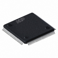
LPC2923FBD100,551 NXP Semiconductors, LPC2923FBD100,551 Datasheet - Page 30

LPC2923FBD100,551
Manufacturer Part Number
LPC2923FBD100,551
Description
IC ARM9 MCU FLASH 256KB 100-LQFP
Manufacturer
NXP Semiconductors
Series
LPC2900r
Datasheet
1.LPC2921FBD100551.pdf
(84 pages)
Specifications of LPC2923FBD100,551
Core Processor
ARM9
Core Size
32-Bit
Speed
125MHz
Connectivity
CAN, I²C, LIN, SPI, UART/USART, USB
Peripherals
DMA, POR, PWM, WDT
Number Of I /o
60
Program Memory Size
256KB (256K x 8)
Program Memory Type
FLASH
Eeprom Size
16K x 8
Ram Size
24K x 8
Voltage - Supply (vcc/vdd)
1.71 V ~ 3.6 V
Data Converters
A/D 16x8b
Oscillator Type
Internal
Operating Temperature
-40°C ~ 85°C
Package / Case
100-LQFP
Processor Series
LPC29
Core
ARM968E-S
3rd Party Development Tools
MDK-ARM, RL-ARM, ULINK2
Lead Free Status / RoHS Status
Lead free / RoHS Compliant
Other names
935287115551
Available stocks
Company
Part Number
Manufacturer
Quantity
Price
Company:
Part Number:
LPC2923FBD100,551
Manufacturer:
NXP Semiconductors
Quantity:
10 000
NXP Semiconductors
LPC2921_23_25_3
Product data sheet
6.13.2.1 Pin description
6.13.2 LIN
6.13.3 I
The LPC2921/2923/2925 contain two LIN 2.0 master controllers. These can be used as
dedicated LIN 2.0 master controllers with additional support for sync break generation and
with hardware implementation of the LIN protocol according to spec 2.0.
The key features are:
The two LIN 2.0 master controllers in the LPC2921/2923/2925 have the pins listed below.
The LIN pins are combined with other functions on the port pins of the
LPC2921/2923/2925.
subsection 3.43, LIN master controller.
Table 18.
Remark: Both LIN channels can be also configured as UART channels.
The LPC2921/2923/2925 each contain two I
The I
(SCL) and a Serial DAta line (SDA). Each device is recognized by a unique address and
can operate as either a receiver-only device (e.g., an LCD driver) or as a transmitter with
the capability to both receive and send information (such as memory). Transmitters and/or
receivers can operate in either master or slave mode, depending on whether the chip has
to initiate a data transfer or is only addressed. The I
controlled by more than one bus master connected to it.
The main features if the I
Symbol
LIN0/1 TXD
LIN0/1 RXD
2
•
•
•
•
•
•
•
•
•
•
•
•
C-bus serial I/O controllers
Complete LIN 2.0 message handling and transfer
One interrupt per LIN message
Slave response time-out detection
Programmable sync-break length
Automatic sync-field and sync-break generation
Programmable inter-byte space
Hardware or software parity generation
Automatic checksum generation
Fault confinement
Fractional baud rate generator
I
and do not support powering off of individual devices connected to the same bus
lines.
Easy to configure as master, slave, or master/slave.
2
2
C0 and I
C-bus is bidirectional for inter-IC control using only two wires: a Serial CLock line
LIN controller pins
Pin name
TXDL0/1
RXDL0/1
2
C1 use standard I/O pins with bit rates of up to 400 kbit/s (Fast I
All information provided in this document is subject to legal disclaimers.
Table 18
Rev. 03 — 14 April 2010
2
C-bus interfaces are:
IN
Direction
OUT
shows the LIN pins. For more information see
ARM9 microcontroller with CAN, LIN, and USB
LIN channel 0/1 receive data input
Description
LIN channel 0/1 transmit data output
2
C-bus controllers.
LPC2921/2923/2925
2
C is a multi-master bus, and it can be
© NXP B.V. 2010. All rights reserved.
Ref. 1
2
C-bus)
30 of 84


