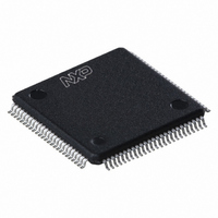
LPC2923FBD100,551 NXP Semiconductors, LPC2923FBD100,551 Datasheet - Page 9

LPC2923FBD100,551
Manufacturer Part Number
LPC2923FBD100,551
Description
IC ARM9 MCU FLASH 256KB 100-LQFP
Manufacturer
NXP Semiconductors
Series
LPC2900r
Datasheet
1.LPC2921FBD100551.pdf
(84 pages)
Specifications of LPC2923FBD100,551
Core Processor
ARM9
Core Size
32-Bit
Speed
125MHz
Connectivity
CAN, I²C, LIN, SPI, UART/USART, USB
Peripherals
DMA, POR, PWM, WDT
Number Of I /o
60
Program Memory Size
256KB (256K x 8)
Program Memory Type
FLASH
Eeprom Size
16K x 8
Ram Size
24K x 8
Voltage - Supply (vcc/vdd)
1.71 V ~ 3.6 V
Data Converters
A/D 16x8b
Oscillator Type
Internal
Operating Temperature
-40°C ~ 85°C
Package / Case
100-LQFP
Processor Series
LPC29
Core
ARM968E-S
3rd Party Development Tools
MDK-ARM, RL-ARM, ULINK2
Lead Free Status / RoHS Status
Lead free / RoHS Compliant
Other names
935287115551
Available stocks
Company
Part Number
Manufacturer
Quantity
Price
Company:
Part Number:
LPC2923FBD100,551
Manufacturer:
NXP Semiconductors
Quantity:
10 000
NXP Semiconductors
Table 3.
[1]
[2]
[3]
[4]
6. Functional description
LPC2921_23_25_3
Product data sheet
Pin name
P0[23]/IN2[7]/
PMAT2[5]/A19
TDI
Bidirectional pad; analog port; plain input; 3-state output; slew rate control; 5 V tolerant; TTL with hysteresis; programmable
pull-up/pull-down/repeater.
USB pad.
Analog pad; analog I/O.
Analog I/O pad.
LQFP100 pin assignment
6.1 Architectural overview
6.2 ARM968E-S processor
Pin
99
100
The LPC2921/2923/2925 consists of:
The LPC2921/2923/2925 configures the ARM968E-S processor in little-endian byte order.
All peripherals run at their own clock frequency to optimize the total system power
consumption. The AHB-to-APB bridge used in the subsystems contains a write-ahead
buffer one transaction deep. This implies that when the ARM968E-S issues a buffered
write action to a register located on the APB side of the bridge, it continues even though
the actual write may not yet have taken place. Completion of a second write to the same
subsystem will not be executed until the first write is finished.
The ARM968E-S is a general purpose 32-bit RISC processor, which offers high
performance and very low power consumption. The ARM architecture is based on
Reduced Instruction Set Computer (RISC) principles, and the instruction set and related
decode mechanism are much simpler than those of microprogrammed Complex
Instruction Set Computers (CISC). This simplicity results in a high instruction throughput
and impressive real-time interrupt response from a small and cost-effective controller
core.
Amongst the most compelling features of the ARM968E-S are:
[4]
•
•
•
•
•
•
[1]
An ARM968E-S processor with real-time emulation support
An AMBA multilayer Advanced High-performance Bus (AHB) for interfacing to the
on-chip memory controllers
Two DTL buses (an universal NXP interface) for interfacing to the interrupt controller
and the Power, Clock and Reset control SubSystem (PCRSS).
Three ARM Peripheral Buses (APB - a compatible super set of ARM's AMBA
advanced peripheral bus) for connection to on-chip peripherals clustered in
subsystems.
One ARM Peripheral Bus for event router and system control.
Separate directly connected instruction and data Tightly Coupled Memory (TCM)
interfaces.
Description
Function 0 (default)
GPIO0, pin 23
IEEE 1149.1 data in, pulled up internally
…continued
All information provided in this document is subject to legal disclaimers.
Rev. 03 — 14 April 2010
Function 1
ADC2 IN7
ARM9 microcontroller with CAN, LIN, and USB
LPC2921/2923/2925
Function 2
PWM2 MAT5
© NXP B.V. 2010. All rights reserved.
Function 3
-
9 of 84


