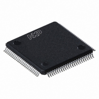
LPC2923FBD100,551 NXP Semiconductors, LPC2923FBD100,551 Datasheet - Page 34

LPC2923FBD100,551
Manufacturer Part Number
LPC2923FBD100,551
Description
IC ARM9 MCU FLASH 256KB 100-LQFP
Manufacturer
NXP Semiconductors
Series
LPC2900r
Datasheet
1.LPC2921FBD100551.pdf
(84 pages)
Specifications of LPC2923FBD100,551
Core Processor
ARM9
Core Size
32-Bit
Speed
125MHz
Connectivity
CAN, I²C, LIN, SPI, UART/USART, USB
Peripherals
DMA, POR, PWM, WDT
Number Of I /o
60
Program Memory Size
256KB (256K x 8)
Program Memory Type
FLASH
Eeprom Size
16K x 8
Ram Size
24K x 8
Voltage - Supply (vcc/vdd)
1.71 V ~ 3.6 V
Data Converters
A/D 16x8b
Oscillator Type
Internal
Operating Temperature
-40°C ~ 85°C
Package / Case
100-LQFP
Processor Series
LPC29
Core
ARM968E-S
3rd Party Development Tools
MDK-ARM, RL-ARM, ULINK2
Lead Free Status / RoHS Status
Lead free / RoHS Compliant
Other names
935287115551
Available stocks
Company
Part Number
Manufacturer
Quantity
Price
Company:
Part Number:
LPC2923FBD100,551
Manufacturer:
NXP Semiconductors
Quantity:
10 000
NXP Semiconductors
LPC2921_23_25_3
Product data sheet
6.14.4.1 Functional description
6.14.3 Clock description
6.14.4 Analog-to-digital converter
Remark: The IDX0 function for the QEI, the external start function for ADC1, and the
TRAP0/1 functions for the PWM0/1 are not pinned out on the LPC2921/2923/2925.
The MSCSS is clocked from a number of different sources:
Each ADC has two clock areas; an APB part clocked by CLK_MSCSS_ADCx_APB (x = 1
or 2) and a control part for the analog section clocked by CLK_ADCx = 1 or 2), see
Section
All clocks are derived from the BASE_MSCSS_CLK, except for CLK_SYS_MSCSS_A
which is derived form BASE_SYS_CLK, and the CLK_ADCx clocks which are derived
from BASE_CLK_ADC. If specific PWM or ADC modules are not used their corresponding
clocks can be switched off.
The MSCSS in the LPC2921/2923/2925 includes two 10-bit successive-approximation
analog-to-digital converters.
The key features of the ADC interface module are:
The ADC block diagram,
functionality is divided into two major parts; one part running on the MSCSS Subsystem
clock, the other on the ADC clock. This split into two clock domains affects the behavior
from a system-level perspective. The actual analog-to-digital conversions take place in the
ADC clock domain, but system control takes place in the system clock domain.
•
•
•
•
•
•
•
•
•
•
•
•
•
CLK_SYS_MSCSS_A clocks the AHB side of the AHB-to-APB bus bridge
CLK_MSCSS_APB clocks the subsystem APB bus
CLK_MSCSS_MTMR0/1 clocks the timers
CLK_MSCSS_PWM[0:3] clocks the PWMs.
ADC1 and ADC2: Eight analog inputs; time-multiplexed; measurement range up to
3.3 V.
External reference-level inputs.
400 ksamples per second at 10-bit resolution up to 1500 ksamples per second at 2-bit
resolution.
Programmable resolution from 2-bit to 10-bit.
Single analog-to-digital conversion scan mode and continuous analog-to-digital
conversion scan mode.
Optional conversion on transition on external start input, timer capture/match signal,
PWM_sync or ‘previous’ ADC.
Converted digital values are stored in a register for each channel.
Optional compare condition to generate a ‘less than’ or an ‘equal to or greater than’
compare-value indication for each channel.
Power-down mode.
6.7.2.
All information provided in this document is subject to legal disclaimers.
Rev. 03 — 14 April 2010
Figure
6, shows the basic architecture of each ADC. The ADC
ARM9 microcontroller with CAN, LIN, and USB
LPC2921/2923/2925
© NXP B.V. 2010. All rights reserved.
34 of 84


