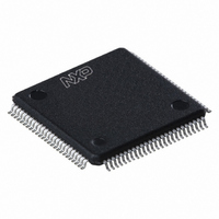
LPC2923FBD100,551 NXP Semiconductors, LPC2923FBD100,551 Datasheet - Page 25

LPC2923FBD100,551
Manufacturer Part Number
LPC2923FBD100,551
Description
IC ARM9 MCU FLASH 256KB 100-LQFP
Manufacturer
NXP Semiconductors
Series
LPC2900r
Datasheet
1.LPC2921FBD100551.pdf
(84 pages)
Specifications of LPC2923FBD100,551
Core Processor
ARM9
Core Size
32-Bit
Speed
125MHz
Connectivity
CAN, I²C, LIN, SPI, UART/USART, USB
Peripherals
DMA, POR, PWM, WDT
Number Of I /o
60
Program Memory Size
256KB (256K x 8)
Program Memory Type
FLASH
Eeprom Size
16K x 8
Ram Size
24K x 8
Voltage - Supply (vcc/vdd)
1.71 V ~ 3.6 V
Data Converters
A/D 16x8b
Oscillator Type
Internal
Operating Temperature
-40°C ~ 85°C
Package / Case
100-LQFP
Processor Series
LPC29
Core
ARM968E-S
3rd Party Development Tools
MDK-ARM, RL-ARM, ULINK2
Lead Free Status / RoHS Status
Lead free / RoHS Compliant
Other names
935287115551
Available stocks
Company
Part Number
Manufacturer
Quantity
Price
Company:
Part Number:
LPC2923FBD100,551
Manufacturer:
NXP Semiconductors
Quantity:
10 000
NXP Semiconductors
LPC2921_23_25_3
Product data sheet
6.12.3.1 Pin description
6.12.3.2 Clock description
6.12.4 UARTs
The timers are designed to count cycles of the clock and optionally generate interrupts or
perform other actions at specified timer values, based on four match registers. They also
include capture inputs to trap the timer value when an input signal changes state,
optionally generating an interrupt. The core function of the timers consists of a 32 bit
prescale counter triggering the 32 bit timer counter. Both counters run on clock
CLK_TMRx (x runs from 0 to 3) and all time references are related to the period of this
clock. Note that each timer has its individual clock source within the Peripheral
SubSystem. In the Modulation and Sampling SubSystem each timer also has its own
individual clock source. See
The four timers in the peripheral subsystem of the LPC2921/2923/2925 have the pins
described below. The two timers in the modulation and sampling subsystem have no
external pins except for the pause pin on MSCSS timer 1. See
description of these timers and their associated pins. The timer pins are combined with
other functions on the port pins of the LPC2921/2923/2925, see
Table 13
Table 13.
[1]
The timer modules are clocked by two different clocks; CLK_SYS_PESS and CLK_TMRx
(x = 0 to 3), see
for power management. The frequency of all these clocks is identical as they are derived
from the same base clock BASE_CLK_TMR. The register interface towards the system
bus is clocked by CLK_SYS_PESS. The timer and prescale counters are clocked by
CLK_TMRx.
The LPC2921/2923/2925 contains two identical UARTs located at different peripheral
base addresses. The key features are:
Symbol
TIMERx CAP[0]
TIMERx CAP[1]
TIMERx CAP[2]
TIMERx CAP[3]
TIMERx MAT[0]
TIMERx MAT[1]
TIMERx MAT[2]
TIMERx MAT[3]
•
•
– Set HIGH on match.
– Toggle on match.
– Do nothing on match.
Pause input pin (MSCSS timers only).
Note that CAP1[0] and CAP1[1] are not pinned out on Timer1.
16-byte receive and transmit FIFOs.
shows the timer pins (x runs from 0 to 3).
Timer pins
All information provided in this document is subject to legal disclaimers.
Section
Pin name
CAPx[0]
CAPx[1]
CAPx[2]
CAPx[3]
MATx[0]
MATx[1]
MATx[2]
MATx[3]
Rev. 03 — 14 April 2010
6.7.2. Note that each timer has its own CLK_TMRx branch clock
Section 6.15.5
Direction
IN
IN
IN
IN
OUT
OUT
OUT
OUT
ARM9 microcontroller with CAN, LIN, and USB
for information on generation of these clocks.
Description
TIMERx capture input 0
TIMERx capture input 1
TIMERx capture input 2
TIMERx capture input 3
TIMERx match output 0
TIMERx match output 1
TIMERx match output 2
TIMERx match output 3
LPC2921/2923/2925
Section 6.14.6
Section
[1]
[1]
© NXP B.V. 2010. All rights reserved.
6.11.3. Table
for a
25 of 84


