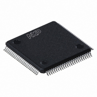
LPC2923FBD100,551 NXP Semiconductors, LPC2923FBD100,551 Datasheet - Page 23

LPC2923FBD100,551
Manufacturer Part Number
LPC2923FBD100,551
Description
IC ARM9 MCU FLASH 256KB 100-LQFP
Manufacturer
NXP Semiconductors
Series
LPC2900r
Datasheet
1.LPC2921FBD100551.pdf
(84 pages)
Specifications of LPC2923FBD100,551
Core Processor
ARM9
Core Size
32-Bit
Speed
125MHz
Connectivity
CAN, I²C, LIN, SPI, UART/USART, USB
Peripherals
DMA, POR, PWM, WDT
Number Of I /o
60
Program Memory Size
256KB (256K x 8)
Program Memory Type
FLASH
Eeprom Size
16K x 8
Ram Size
24K x 8
Voltage - Supply (vcc/vdd)
1.71 V ~ 3.6 V
Data Converters
A/D 16x8b
Oscillator Type
Internal
Operating Temperature
-40°C ~ 85°C
Package / Case
100-LQFP
Processor Series
LPC29
Core
ARM968E-S
3rd Party Development Tools
MDK-ARM, RL-ARM, ULINK2
Lead Free Status / RoHS Status
Lead free / RoHS Compliant
Other names
935287115551
Available stocks
Company
Part Number
Manufacturer
Quantity
Price
Company:
Part Number:
LPC2923FBD100,551
Manufacturer:
NXP Semiconductors
Quantity:
10 000
NXP Semiconductors
LPC2921_23_25_3
Product data sheet
6.11.4.1 Pin description
6.12.1 Peripheral subsystem clock description
6.12.2 Watchdog timer
6.12 Peripheral subsystem
The event router module in the LPC2921/2923/2925 is connected to the pins listed below.
The pins are combined with other functions on the port pins of the LPC2921/2923/2925.
Table 12
Table 12.
The peripheral subsystem is clocked by a number of different clocks:
The purpose of the watchdog timer is to reset the ARM9 processor within a reasonable
amount of time if the processor enters an error state. The watchdog generates a system
reset if the user program fails to trigger it correctly within a predetermined amount of time.
Key features:
Symbol
EXTINT[0:3]
CAN0 RXD
CAN1 RXD
I2C0_SCL
I2C1_SCL
LIN0 RXD
LIN1 RXD
SPI0 SDI
SPI1 SDI
SPI2 SDI
UART0 RXD
UART1 RXD
-
-
-
•
•
•
•
•
•
•
•
•
CLK_SYS_PESS
CLK_UART0/1
CLK_SPI0/1/2
CLK_TMR0/1/2/3
CLK_SAFE see
Internal chip reset if not periodically triggered
Timer counter register runs on always-on safe clock
Optional interrupt generation on watchdog time-out
Debug mode with disabling of reset
shows the pins connected to the event router.
Event-router pin connections
All information provided in this document is subject to legal disclaimers.
Direction
I
I
I
I
I
I
I
I
I
I
I
I
n/a
n/a
n/a
Section 6.7.2
Rev. 03 — 14 April 2010
Description
external interrupt inputs 0 to 3
CAN0 receive data input wake-up
CAN1 receive data input wake-up
I
I
LIN0 receive data input wake-up
LIN1 receive data input wake-up
SPI0 receive data input
SPI1 receive data input
SPI2 receive data input
UART0 receive data input
UART1 receive data input
CAN interrupt (internal)
VIC FIQ (internal)
VIC IRQ (internal)
2
2
C0 SCL clock input
C1 SCL clock input
ARM9 microcontroller with CAN, LIN, and USB
LPC2921/2923/2925
© NXP B.V. 2010. All rights reserved.
Default polarity
1
0
0
0
0
0
0
0
0
0
0
0
1
1
1
23 of 84


