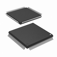
M3062GF8NGP#U5 Renesas Electronics America, M3062GF8NGP#U5 Datasheet - Page 137

M3062GF8NGP#U5
Manufacturer Part Number
M3062GF8NGP#U5
Description
MCU 3V 64K PB FREE 100-LQFP
Manufacturer
Renesas Electronics America
Series
M16C™ M16C/60r
Datasheet
1.M3062GF8NGPD5.pdf
(243 pages)
Specifications of M3062GF8NGP#U5
Core Processor
M16C/60
Core Size
16-Bit
Speed
10MHz
Connectivity
SIO, UART/USART
Peripherals
DMA, WDT
Number Of I /o
85
Program Memory Size
64KB (64K x 8)
Program Memory Type
FLASH
Ram Size
8K x 8
Voltage - Supply (vcc/vdd)
2.7 V ~ 3.6 V
Data Converters
A/D 10x10b, D/A 2x8b
Oscillator Type
Internal
Operating Temperature
-20°C ~ 85°C
Package / Case
100-LQFP
Lead Free Status / RoHS Status
Lead free / RoHS Compliant
Eeprom Size
-
Available stocks
Company
Part Number
Manufacturer
Quantity
Price
Part Number:
M3062GF8NGP#U5M3062GF8NGP#D5
Manufacturer:
Renesas Electronics America
Quantity:
10 000
UART2 Special Mode Register
134
Rev.1.1
Figure 1.16.26. UART2 special mode register
UART2 Special Mode Register
The UART2 special mode register (address 0377
Figure 1.16.26 shows the UART2 special mode register.
Bit 0 of the UART2 special mode register (0377
Setting “1” in the I
interface effective.
Table 1.16.9 shows the relation between the I
Since this function uses clock-synchronous serial I/O mode, set this bit to “0” in UART mode.
UART2 special mode register 3 (I C bus exclusive use register)
b7 b6 b5 b4 b3 b2 b1 b0
UART2 special mode register
Note 1: This bit can be read or written to when UART2 special mode register (U2SMR at address 0377
Note 2: These bits are initialized to “000” when SDDS = “0”. After a reset, these bits are set to “000”. However,
Note 3: The amount of delay varies with the load on SCL and SDA pins. Also, when using an external clock, the
b7 b6 b5 b4 b3 b2 b1 b0
7 (SDDS: SDA digital delay select bit) = “1”. When the initial value of UART2 special mode register 3
(U2SMR3) is read after setting SDDS = “1”, the value is “00
register 3 (U2SMR3) after setting SDDS = “1”, be sure to write 0's to bits 0–4. When SDDS = “0”,
this register cannot be written to; when read, the value is indeterminate.
because these bits can be read only when SDDS = “1”, the value read from these bits when SDDS = “0”
is indeterminate.
amount of delay increases by about 200 ns, so be sure to take this into account when using the device.
2
C mode select bit (bit 0) goes the circuit to achieve the I
Note 1: Nothing but “0” may be written.
Note 2: When not in I
Note 3: When analog delay is selected, only the analog delay value is effective; when digital delay is selected,
ABSCS
ACSE
symbol
SSS
SDDS
LSYN
DL0
DL1
DL2
IICM
ABC
BBS
Nothing is assigned.
In an attempt to write to these bits, write “0”. The value, if read, turns out to be
indeterminate. However, when SDDS = “1”, the value “0” is read out (Note 1)
symbol
Bit
Bit
bit = “0”, UART2 special mode register 3 (U2SMR3 at address 0375
digital delay setup bits) are initialized to “000”, with the analog delay circuit selected. Also, when SDDS
only the digital delay value is effective.
Symbol
U2SMR
= “0”, the U2SMR3 register cannot be read or written to.
Symbol
I
Arbitration lost detecting
flag control bit
Transmit start condition
select bit
SDA digital delay select
bit (Note 2, Note 3)
Bus busy flag
SCL L sync output
enable bit
Bus collision detect
sampling clock select bit
Auto clear function
select bit of transmit
enable bit
U2SMR3
2
C mode select bit
SDA digital delay setup
bit
(Note 1, Note 2, Note 3)
2
name
2
C mode, do not set this bit by writing a “1”. During normal mode, fix it to “0”. When this
Bit name
Bit
Address
0377
Address
0375
16
0 : STOP condition detected
1 : START condition detected
0 : Analog delay output
1 : Digital delay output
(must always be “0” when
(During clock synchronous
0 : Normal mode
1 : I
0 : Update per bit
1 : Update per byte
0 : Disabled
1 : Enabled
Must always be “0”
Must always be “0”
Must always be “0”
not using I C mode)
2
16
is selected
is selected
C mode select bit and respective control workings.
2
C mode
b7 b6 b5
16
serial I/O mode)
0 0 0 : Must not be set when using I
0 0 1 : 1 to 2 cycle(s) of 1/f(X
0 1 0 : 2 to 3 cycles of 1/f(X
0 1 1 : 3 to 4 cycles of 1/f(X
1 0 0 : 4 to 5 cycles of 1/f(X
1 0 1 : 5 to 6 cycles of 1/f(X
1 1 0 : 6 to 7 cycles of 1/f(X
1 1 1 : 7 to 8 cycles of 1/f(X
When reset
16
) is used as the I
Function
00
2
) is used to control UART2 in various ways.
When reset
16
(I C bus exclusive use register)
00
16
2
16
”. When writing to UART2 special mode
0 : Rising edge of transfer
1 : Underflow signal of timer A0
0 : Ordinary
1 : Falling edge of RxD
Function
0 : No auto clear function
1 : Auto clear at occurrence of
Must always be “0”
Must always be “0”
Must always be “0”
Must always be “0”
Must always be “0”
clock
bus collision
(During UART mode)
IN
IN
IN
IN
IN
IN
16
IN
)
)
)
)
)
)
) bits 7 to 5 (DL2 to DL0 = SDA
Function
SINGLE-CHIP 16-BIT CMOS MICROCOMPUTER
)
2
C mode select bit.
2
C mode
Digital delay
is selected
2
2
16
(Note1)
R
C bus (simplified I
) bit
R
W
W
M3062GF8NFP/GP
Mitsubishi microcomputers
2
C bus)


