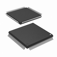
M3062GF8NGP#U5 Renesas Electronics America, M3062GF8NGP#U5 Datasheet - Page 191

M3062GF8NGP#U5
Manufacturer Part Number
M3062GF8NGP#U5
Description
MCU 3V 64K PB FREE 100-LQFP
Manufacturer
Renesas Electronics America
Series
M16C™ M16C/60r
Datasheet
1.M3062GF8NGPD5.pdf
(243 pages)
Specifications of M3062GF8NGP#U5
Core Processor
M16C/60
Core Size
16-Bit
Speed
10MHz
Connectivity
SIO, UART/USART
Peripherals
DMA, WDT
Number Of I /o
85
Program Memory Size
64KB (64K x 8)
Program Memory Type
FLASH
Ram Size
8K x 8
Voltage - Supply (vcc/vdd)
2.7 V ~ 3.6 V
Data Converters
A/D 10x10b, D/A 2x8b
Oscillator Type
Internal
Operating Temperature
-20°C ~ 85°C
Package / Case
100-LQFP
Lead Free Status / RoHS Status
Lead free / RoHS Compliant
Eeprom Size
-
Available stocks
Company
Part Number
Manufacturer
Quantity
Price
Part Number:
M3062GF8NGP#U5M3062GF8NGP#D5
Manufacturer:
Renesas Electronics America
Quantity:
10 000
Rev.1.1
Mitsubishi microcomputers
M3062GF8NFP/GP
CPU Rewrite Mode (Flash Memory Version)
SINGLE-CHIP 16-BIT CMOS MICROCOMPUTER
Outline Performance (CPU Rewrite Mode)
In the CPU rewrite mode, the CPU erases, programs and reads the internal flash memory as instructed by
software commands. Operations must be executed from a memory other than the internal flash memory,
such as the internal RAM.
When the CPU rewrite mode select bit (bit 1 at address 03B7
) is set to “1”, transition to CPU rewrite mode
16
occurs and software commands can be accepted.
In the CPU rewrite mode, write to and read from software commands and data into even-numbered ad-
dress (“0” for byte address A0) in 16-bit units. Write data into even address in 16-bit units. Do not write 16-
bit data into odd address or data in 8-bit units. Always write 8-bit software commands into even-numbered
address. Commands are ignored with odd-numbered addresses.
Use software commands to control program and erase operations. Whether a program or erase operation
has terminated normally or in error can be verified by reading the status register. Read data from an even
address in the user ROM area when reading the status register.
Figure 1.29.1 shows the flash identification register and flash memory control register 0.
_____
Bit 0 of the flash memory control register 0 is the RY/BY status flag used exclusively to read the operating
status of the flash memory. During programming, erase and lock-bit programming operations, it is “0”.
Otherwise, it is “1”.
Bit 1 of the flash memory control register 0 is the CPU rewrite mode select bit. The CPU rewrite mode is
entered by setting this bit to “1”, so that software commands become acceptable. In CPU rewrite mode, the
CPU becomes unable to access the internal flash memory directly. Therefore, Write to this bit only when
_______
executing out of an area other than the internal flash memory. Also only when NMI pin is "H" level. To set
this bit to “1”, it is necessary to write “0” and then write “1” in succession. To set this bit to “0” by only writing
a “0” .
Bit 2 of the flash memory control register 0 is a lock bit disable select bit. By setting this bit to “1”, it is
possible to disable erase and write protect (block lock) effectuated by the lock bit data. The lock bit disable
select bit only disables the lock bit function; it does not change the lock data bit value. However, if an erase
operation is performed when this bit =“1”, the lock bit data that is “0” (locked) is set to “1” (unlocked) after
erasure. To set this bit to “1”, it is necessary to write “0” and then write “1” in succession. This bit can be
manipulated only when the CPU rewrite mode select bit = “1”.
Bit 3 of the flash memory control register 0 is the flash memory reset bit used to reset the control circuit of
the internal flash memory. This bit is used when exiting CPU rewrite mode and when flash memory access
has failed. When the CPU rewrite mode select bit is “1”, writing “1” for this bit resets the control circuit. To
_____
release the reset, it is necessary to set this bit to “0” when RY/BY status flag is “1”.
Bit 5 of the flash memory control register 0 is a user ROM area select bit which is effective in only boot
mode. If this bit is set to “1” in boot mode, the area to be accessed is switched from the boot ROM area to
the user ROM area. When the CPU rewrite mode needs to be used in boot mode, set this bit to “1”. Note
that if the microcomputer is booted from the user ROM area, it is always the user ROM area that can be
accessed and this bit has no effect. When in boot mode, the function of this bit is effective regardless of
whether the CPU rewrite mode is on or off. Write to this bit only when executing out of an area other than
the internal flash memory.
Bit 6 of the flash memory control register 0 is the program status flag used exclusively to read the operating
status of the auto program operation. If a program error occurs, it is set to “1”. Otherwise, it is “0”.
Bit 7 of the flash memory control register 0 is the erase status flag used exclusively to read the operating
status of the auto erase operation. If an erase error occurs, it is set to “1”. Otherwise, it is “0”.
188


