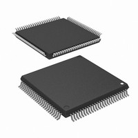
M3062GF8NGP#U5 Renesas Electronics America, M3062GF8NGP#U5 Datasheet - Page 194

M3062GF8NGP#U5
Manufacturer Part Number
M3062GF8NGP#U5
Description
MCU 3V 64K PB FREE 100-LQFP
Manufacturer
Renesas Electronics America
Series
M16C™ M16C/60r
Datasheet
1.M3062GF8NGPD5.pdf
(243 pages)
Specifications of M3062GF8NGP#U5
Core Processor
M16C/60
Core Size
16-Bit
Speed
10MHz
Connectivity
SIO, UART/USART
Peripherals
DMA, WDT
Number Of I /o
85
Program Memory Size
64KB (64K x 8)
Program Memory Type
FLASH
Ram Size
8K x 8
Voltage - Supply (vcc/vdd)
2.7 V ~ 3.6 V
Data Converters
A/D 10x10b, D/A 2x8b
Oscillator Type
Internal
Operating Temperature
-20°C ~ 85°C
Package / Case
100-LQFP
Lead Free Status / RoHS Status
Lead free / RoHS Compliant
Eeprom Size
-
Available stocks
Company
Part Number
Manufacturer
Quantity
Price
Part Number:
M3062GF8NGP#U5M3062GF8NGP#D5
Manufacturer:
Renesas Electronics America
Quantity:
10 000
- Current page: 194 of 243
- Download datasheet (4Mb)
CPU Rewrite Mode (Flash Memory Version)
Rev.1.1
Precautions on CPU Rewrite Mode
Described below are the precautions to be observed when rewriting the flash memory in CPU rewrite mode.
(1) Operation speed
(2) Instructions inhibited against use
(3) Interrupts inhibited against use
(4) Access disable
(5) How to access
(6)Writing in the user ROM area
(7)Using the lock bit
During CPU rewrite mode, set the BCLK as shown below using the main clock divide ratio select bit
(bit 6 at address 0006
6.25 MHz or less when wait bit (bit 7 at address 0005
10.0 MHz or less when wait bit (bit 7 at address 0005
The instructions listed below cannot be used during CPU rewrite mode because they refer to the
internal data of the flash memory:
UND instruction, INTO instruction, JMPS instruction, JSRS instruction, and BRK instruction
The address match interrupt cannot be used during CPU rewrite mode because they refer to the
internal data of the flash memory. If interrupts have their vector in the variable vector table, they can be
used by transferring the vector into the RAM area. The NMI and watchdog timer interrupts can be
used to automatically initialize the flash identification register and flash memory control register 0 to
“0”, then return to normal operation. However, these two interrupts' jump addresses are located in the
fixed vector table and there must exsist a routine to be executed. Since the rewrite operation is halted
when an NMI or watchdog timer interrupts occurs, you must reset the CPU rewite mode select bit to
“1” and the perform the erase/program operation again.
Write to CPU rewrite mode select bit and user ROM area select bit only when executing out of an area
other than the internal flash memory.
For CPU rewrite mode select bit and lock bit disable select bit to be set to “1”, the user needs to write
a “0” and then a “1” to it in succession. When it is not this procedure, it is not enacted in “1”. This is
necessary to ensure that no interrupt or DMA transfer will be executed during the interval. Write to
CPU rewrite mode select bit and user ROM area select bit only when executing out of an area other
than the internal flash memory.Also only when NMI pin is “H” level.
If power is lost while rewriting blocks that contain the flash rewrite program with the CPU rewrite mode,
those blocks may not be correctly rewritten and it is possible that the flash memory can no longer be
rewritten after that. Therefore, it is recommended to use the standard serial I/O mode or parallel I/O
mode to rewrite these blocks.
To use the CPU rewrite mode, use a boot program that can set and cancel the lock command.
_______
16
and bits 6 and 7 at address 0007
_______
16
16
) = 0 (without internal access wait state)
) = 1 (with internal access wait state)
_______
16
):
SINGLE-CHIP 16-BIT CMOS MICROCOMPUTER
M3062GF8NFP/GP
Mitsubishi microcomputers
191
Related parts for M3062GF8NGP#U5
Image
Part Number
Description
Manufacturer
Datasheet
Request
R

Part Number:
Description:
KIT STARTER FOR M16C/29
Manufacturer:
Renesas Electronics America
Datasheet:

Part Number:
Description:
KIT STARTER FOR R8C/2D
Manufacturer:
Renesas Electronics America
Datasheet:

Part Number:
Description:
R0K33062P STARTER KIT
Manufacturer:
Renesas Electronics America
Datasheet:

Part Number:
Description:
KIT STARTER FOR R8C/23 E8A
Manufacturer:
Renesas Electronics America
Datasheet:

Part Number:
Description:
KIT STARTER FOR R8C/25
Manufacturer:
Renesas Electronics America
Datasheet:

Part Number:
Description:
KIT STARTER H8S2456 SHARPE DSPLY
Manufacturer:
Renesas Electronics America
Datasheet:

Part Number:
Description:
KIT STARTER FOR R8C38C
Manufacturer:
Renesas Electronics America
Datasheet:

Part Number:
Description:
KIT STARTER FOR R8C35C
Manufacturer:
Renesas Electronics America
Datasheet:

Part Number:
Description:
KIT STARTER FOR R8CL3AC+LCD APPS
Manufacturer:
Renesas Electronics America
Datasheet:

Part Number:
Description:
KIT STARTER FOR RX610
Manufacturer:
Renesas Electronics America
Datasheet:

Part Number:
Description:
KIT STARTER FOR R32C/118
Manufacturer:
Renesas Electronics America
Datasheet:

Part Number:
Description:
KIT DEV RSK-R8C/26-29
Manufacturer:
Renesas Electronics America
Datasheet:

Part Number:
Description:
KIT STARTER FOR SH7124
Manufacturer:
Renesas Electronics America
Datasheet:

Part Number:
Description:
KIT STARTER FOR H8SX/1622
Manufacturer:
Renesas Electronics America
Datasheet:

Part Number:
Description:
KIT DEV FOR SH7203
Manufacturer:
Renesas Electronics America
Datasheet:


