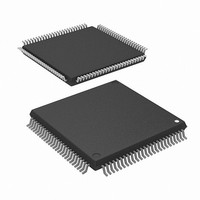
M3062GF8NGP#U5 Renesas Electronics America, M3062GF8NGP#U5 Datasheet - Page 163

M3062GF8NGP#U5
Manufacturer Part Number
M3062GF8NGP#U5
Description
MCU 3V 64K PB FREE 100-LQFP
Manufacturer
Renesas Electronics America
Series
M16C™ M16C/60r
Datasheet
1.M3062GF8NGPD5.pdf
(243 pages)
Specifications of M3062GF8NGP#U5
Core Processor
M16C/60
Core Size
16-Bit
Speed
10MHz
Connectivity
SIO, UART/USART
Peripherals
DMA, WDT
Number Of I /o
85
Program Memory Size
64KB (64K x 8)
Program Memory Type
FLASH
Ram Size
8K x 8
Voltage - Supply (vcc/vdd)
2.7 V ~ 3.6 V
Data Converters
A/D 10x10b, D/A 2x8b
Oscillator Type
Internal
Operating Temperature
-20°C ~ 85°C
Package / Case
100-LQFP
Lead Free Status / RoHS Status
Lead free / RoHS Compliant
Eeprom Size
-
Available stocks
Company
Part Number
Manufacturer
Quantity
Price
Part Number:
M3062GF8NGP#U5M3062GF8NGP#D5
Manufacturer:
Renesas Electronics America
Quantity:
10 000
- Current page: 163 of 243
- Download datasheet (4Mb)
Programmable I/O Port
160
Rev.1.1
Programmable I/O Ports
There are 87 programmable I/O ports: P0 to P10 (excluding P8
input or output using the direction register. A pull-up resistance for each block of 4 ports can be set. P8
an input-only port and has no built-in pull-up resistance.
Figures 1.20.1 to 1.20.4 show the programmable I/O ports. Figure 1.20.5 shows the I/O pins.
Each pin functions as a programmable I/O port and as the I/O for the built-in peripheral devices.
To use the pins as the inputs for the built-in peripheral devices, set the direction register of each pin to input
mode. When the pins are used as the outputs for the built-in peripheral devices (other than the D-A con-
verter), they function as outputs regardless of the contents of the direction registers. When pins are to be
used as the outputs for the D-A converter, do not set the direction registers to output mode. See the
descriptions of the respective functions for how to set up the built-in peripheral devices.
(1) Direction registers
(2) Port registers
(3) Pull-up control registers
(4) Port control register
Figure 1.20.6 shows the direction registers.
These registers are used to choose the direction of the programmable I/O ports. Each bit in these regis-
ters corresponds one for one to each I/O pin.
In memory expansion and microprocessor mode, the contents of corresponding direction register of pins
A
be modified.
Note: There is no direction register bit for P8
Figure 1.20.7 shows the port registers.
These registers are used to write and read data for input and output to and from an external device. A
port register consists of a port latch to hold output data and a circuit to read the status of a pin. Each bit
in port registers corresponds one for one to each I/O pin.
In memory expansion and microprocessor mode, the contents of corresponding port register of pins A
A
modified.
Figure 1.20.8 shows the pull-up control registers.
The pull-up control register can be set to apply a pull-up resistance to each block of 4 ports. When ports
are set to have a pull-up resistance, the pull-up resistance is connected only when the direction register is
set for input.
However, in memory expansion mode and microprocessor mode, the pull-up control register of P0 to P3,
P4
connected.
Figure 1.20.9 shows the port control register.
The bit 0 of port control register is used to read port P1 as follows:
This register is valid in the following:
0
19
0
to A
0 : When port P1 is input port, port input level is read.
1 : The contents of port P1 register is read always.
• External bus width is 8 bits in microprocessor mode or memory expansion mode.
• Port P1 can be used as a port in multiplexed bus for the entire space.
, D
to P4
0
When port P1 is output port , the contents of port P1 register is read.
19
to D
, D
3
, and P5 is invalid. The contents of register can be changed, but the pull-up resistance is not
0
15
to D
, CS0 to CS3, RD, WRL/WR, WRH/BHE, ALE, RDY, HOLD, HLDA and BCLK cannot be
_______
15
, CS0 to CS3, RD, WRL/WR, WRH/BHE, ALE, RDY, HOLD, HLDA and BCLK cannot
_______
________ _____
_______
________ ______
_____
________ ______
5
________ ________
.
________ _______
5
_______
). Each port can be set independently for
SINGLE-CHIP 16-BIT CMOS MICROCOMPUTER
_______
__________
__________
_________
_________
M3062GF8NFP/GP
Mitsubishi microcomputers
0
5
to
is
Related parts for M3062GF8NGP#U5
Image
Part Number
Description
Manufacturer
Datasheet
Request
R

Part Number:
Description:
KIT STARTER FOR M16C/29
Manufacturer:
Renesas Electronics America
Datasheet:

Part Number:
Description:
KIT STARTER FOR R8C/2D
Manufacturer:
Renesas Electronics America
Datasheet:

Part Number:
Description:
R0K33062P STARTER KIT
Manufacturer:
Renesas Electronics America
Datasheet:

Part Number:
Description:
KIT STARTER FOR R8C/23 E8A
Manufacturer:
Renesas Electronics America
Datasheet:

Part Number:
Description:
KIT STARTER FOR R8C/25
Manufacturer:
Renesas Electronics America
Datasheet:

Part Number:
Description:
KIT STARTER H8S2456 SHARPE DSPLY
Manufacturer:
Renesas Electronics America
Datasheet:

Part Number:
Description:
KIT STARTER FOR R8C38C
Manufacturer:
Renesas Electronics America
Datasheet:

Part Number:
Description:
KIT STARTER FOR R8C35C
Manufacturer:
Renesas Electronics America
Datasheet:

Part Number:
Description:
KIT STARTER FOR R8CL3AC+LCD APPS
Manufacturer:
Renesas Electronics America
Datasheet:

Part Number:
Description:
KIT STARTER FOR RX610
Manufacturer:
Renesas Electronics America
Datasheet:

Part Number:
Description:
KIT STARTER FOR R32C/118
Manufacturer:
Renesas Electronics America
Datasheet:

Part Number:
Description:
KIT DEV RSK-R8C/26-29
Manufacturer:
Renesas Electronics America
Datasheet:

Part Number:
Description:
KIT STARTER FOR SH7124
Manufacturer:
Renesas Electronics America
Datasheet:

Part Number:
Description:
KIT STARTER FOR H8SX/1622
Manufacturer:
Renesas Electronics America
Datasheet:

Part Number:
Description:
KIT DEV FOR SH7203
Manufacturer:
Renesas Electronics America
Datasheet:


