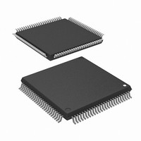
M3062GF8NGP#U5 Renesas Electronics America, M3062GF8NGP#U5 Datasheet - Page 193

M3062GF8NGP#U5
Manufacturer Part Number
M3062GF8NGP#U5
Description
MCU 3V 64K PB FREE 100-LQFP
Manufacturer
Renesas Electronics America
Series
M16C™ M16C/60r
Datasheet
1.M3062GF8NGPD5.pdf
(243 pages)
Specifications of M3062GF8NGP#U5
Core Processor
M16C/60
Core Size
16-Bit
Speed
10MHz
Connectivity
SIO, UART/USART
Peripherals
DMA, WDT
Number Of I /o
85
Program Memory Size
64KB (64K x 8)
Program Memory Type
FLASH
Ram Size
8K x 8
Voltage - Supply (vcc/vdd)
2.7 V ~ 3.6 V
Data Converters
A/D 10x10b, D/A 2x8b
Oscillator Type
Internal
Operating Temperature
-20°C ~ 85°C
Package / Case
100-LQFP
Lead Free Status / RoHS Status
Lead free / RoHS Compliant
Eeprom Size
-
Available stocks
Company
Part Number
Manufacturer
Quantity
Price
Part Number:
M3062GF8NGP#U5M3062GF8NGP#D5
Manufacturer:
Renesas Electronics America
Quantity:
10 000
- Current page: 193 of 243
- Download datasheet (4Mb)
190
CPU Rewrite Mode (Flash Memory Version)
Rev.1.1
Figure 1.29.2. CPU rewrite mode set/reset flowchart
Note 1: During CPU rewrite mode, set the BCLK as shown below using the main clock divide ratio select bit (bit 6
Note 2: For CPU rewrite mode select bit to be set to “1”, the user needs to write a “0” and then a “1” to it in
Note 3: Before exiting the CPU rewrite mode after completing erase or program operation, always be sure to
Note 4: “1” can be set. However, when this bit is “1”, user ROM area is accessed.
(Subsequent operations are executed by control
Jump to transferred control program in RAM
Single-chip mode, memory expansion
Set processor mode register (Note 1)
at address 0006
6.25 MHz or less when wait bit (bit 7 at address 0005
10.0 MHz or less when wait bit (bit 7 at address 0005
succession. When it is not this procedure, it is not enacted in “1”. This is necessary to ensure that no
interrupt or DMA transfer will be executed during the interval. Write to this bit only when executing out of
an area other than the internal flash memory. Also only when NMI pin is “H” level.
execute a read array command or reset the flash memory.
Transfer CPU rewrite mode control
program to internal RAM
program in this RAM)
Program in ROM
mode, or boot mode
Start
16
*1
and bits 6 and 7 at address 0007
16
16
16
):
Execute read array command or reset flash
memory by setting flash memory reset bit (by
writing “1” and then “0” in succession) (Note 3)
) = “0” (without internal access wait state)
) = “1” (with internal access wait state)
Set CPU rewrite mode select bit to “1” (by
writing “0” and then “1” in succession)(Note 2)
(Boot mode only)
Write “0” to user ROM area select bit (Note 4)
Using software command execute erase,
program, or other operation
(Set lock bit disable bit as required)
Write “0” to CPU rewrite mode select bit
(Boot mode only)
Set user ROM area select bit to “1”
Program in RAM
SINGLE-CHIP 16-BIT CMOS MICROCOMPUTER
End
*1
M3062GF8NFP/GP
Mitsubishi microcomputers
Related parts for M3062GF8NGP#U5
Image
Part Number
Description
Manufacturer
Datasheet
Request
R

Part Number:
Description:
KIT STARTER FOR M16C/29
Manufacturer:
Renesas Electronics America
Datasheet:

Part Number:
Description:
KIT STARTER FOR R8C/2D
Manufacturer:
Renesas Electronics America
Datasheet:

Part Number:
Description:
R0K33062P STARTER KIT
Manufacturer:
Renesas Electronics America
Datasheet:

Part Number:
Description:
KIT STARTER FOR R8C/23 E8A
Manufacturer:
Renesas Electronics America
Datasheet:

Part Number:
Description:
KIT STARTER FOR R8C/25
Manufacturer:
Renesas Electronics America
Datasheet:

Part Number:
Description:
KIT STARTER H8S2456 SHARPE DSPLY
Manufacturer:
Renesas Electronics America
Datasheet:

Part Number:
Description:
KIT STARTER FOR R8C38C
Manufacturer:
Renesas Electronics America
Datasheet:

Part Number:
Description:
KIT STARTER FOR R8C35C
Manufacturer:
Renesas Electronics America
Datasheet:

Part Number:
Description:
KIT STARTER FOR R8CL3AC+LCD APPS
Manufacturer:
Renesas Electronics America
Datasheet:

Part Number:
Description:
KIT STARTER FOR RX610
Manufacturer:
Renesas Electronics America
Datasheet:

Part Number:
Description:
KIT STARTER FOR R32C/118
Manufacturer:
Renesas Electronics America
Datasheet:

Part Number:
Description:
KIT DEV RSK-R8C/26-29
Manufacturer:
Renesas Electronics America
Datasheet:

Part Number:
Description:
KIT STARTER FOR SH7124
Manufacturer:
Renesas Electronics America
Datasheet:

Part Number:
Description:
KIT STARTER FOR H8SX/1622
Manufacturer:
Renesas Electronics America
Datasheet:

Part Number:
Description:
KIT DEV FOR SH7203
Manufacturer:
Renesas Electronics America
Datasheet:


