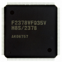
DF61657CN35FTV Renesas Electronics America, DF61657CN35FTV Datasheet - Page 178

DF61657CN35FTV
Manufacturer Part Number
DF61657CN35FTV
Description
IC H8SX/1657 MCU FLASH 120TQFP
Manufacturer
Renesas Electronics America
Series
H8® H8SX/1600r
Datasheet
1.DF61656N35FTV.pdf
(894 pages)
Specifications of DF61657CN35FTV
Core Processor
H8SX
Core Size
32-Bit
Speed
35MHz
Connectivity
SCI, SmartCard
Peripherals
DMA, PWM, WDT
Number Of I /o
82
Program Memory Size
768KB (768K x 8)
Program Memory Type
FLASH
Ram Size
24K x 8
Voltage - Supply (vcc/vdd)
3 V ~ 3.6 V
Data Converters
A/D 8x10b; D/A 2x8b
Oscillator Type
Internal
Operating Temperature
-20°C ~ 75°C
Package / Case
120-TQFP, 120-VQFP
For Use With
3DK1657 - DEV EVAL KIT FOR H8SX/1657
Lead Free Status / RoHS Status
Lead free / RoHS Compliant
Eeprom Size
-
Available stocks
Company
Part Number
Manufacturer
Quantity
Price
Company:
Part Number:
DF61657CN35FTV
Manufacturer:
RENESAS
Quantity:
101
Company:
Part Number:
DF61657CN35FTV
Manufacturer:
Renesas Electronics America
Quantity:
10 000
- Current page: 178 of 894
- Download datasheet (5Mb)
Section 6 Bus Controller (BSC)
6.2.12
MPXCR specifies the address/data multiplexed I/O interface.
When the bus interface of each area in the external address space is specified as a basic interface
or a byte control SRAM interface, the MPXCR setting has priority over the SRAMCR setting and
the SRAMCR setting is invalid.
Rev. 2.00 Jun. 28, 2007 Page 152 of 864
REJ09B0341-0200
Bit
15
14
13
12
11
10 to 1
0
Bit
Bit Name
Initial Value
R/W
Bit
Bit Name
Initial Value
R/W
Bit Name
MPXE7
MPXE6
MPXE5
MPXE4
MPXE3
ADDEX
Address/Data Multiplexed I/O Control Register (MPXCR)
MPXE7
R/W
15
R
0
7
0
Initial
Value
0
0
0
0
0
All 0
0
MPXE6
R/W
14
R
0
6
0
R/W
R/W
R/W
R/W
R/W
R/W
R
R/W
MPXE5
R/W
13
R
0
5
0
Description
Address/Data Multiplexed I/O Interface Select
Specifies the bus interface for the corresponding area.
To set this bit to 1, clear the BCSELn bit in SRAMCR to
0.
0: Area n is specified as a basic interface or a byte
1: Area n is specified as an address/data multiplexed I/O
(n = 7 to 3)
Reserved
These are read-only bits and cannot be modified.
Address Output Cycle Extension
Specifies whether a wait cycle is inserted for the address
output cycle of address/data multiplexed I/O interface.
0: No wait cycle is inserted for the address output cycle
1: One wait cycle is inserted for the address output cycle
control SRAM interface.
interface
MPXE4
R/W
12
R
0
4
0
MPXE3
R/W
11
R
0
3
0
10
R
R
0
2
0
R
R
9
0
1
0
ADDEX
R/W
R
8
0
0
0
Related parts for DF61657CN35FTV
Image
Part Number
Description
Manufacturer
Datasheet
Request
R

Part Number:
Description:
KIT STARTER FOR M16C/29
Manufacturer:
Renesas Electronics America
Datasheet:

Part Number:
Description:
KIT STARTER FOR R8C/2D
Manufacturer:
Renesas Electronics America
Datasheet:

Part Number:
Description:
R0K33062P STARTER KIT
Manufacturer:
Renesas Electronics America
Datasheet:

Part Number:
Description:
KIT STARTER FOR R8C/23 E8A
Manufacturer:
Renesas Electronics America
Datasheet:

Part Number:
Description:
KIT STARTER FOR R8C/25
Manufacturer:
Renesas Electronics America
Datasheet:

Part Number:
Description:
KIT STARTER H8S2456 SHARPE DSPLY
Manufacturer:
Renesas Electronics America
Datasheet:

Part Number:
Description:
KIT STARTER FOR R8C38C
Manufacturer:
Renesas Electronics America
Datasheet:

Part Number:
Description:
KIT STARTER FOR R8C35C
Manufacturer:
Renesas Electronics America
Datasheet:

Part Number:
Description:
KIT STARTER FOR R8CL3AC+LCD APPS
Manufacturer:
Renesas Electronics America
Datasheet:

Part Number:
Description:
KIT STARTER FOR RX610
Manufacturer:
Renesas Electronics America
Datasheet:

Part Number:
Description:
KIT STARTER FOR R32C/118
Manufacturer:
Renesas Electronics America
Datasheet:

Part Number:
Description:
KIT DEV RSK-R8C/26-29
Manufacturer:
Renesas Electronics America
Datasheet:

Part Number:
Description:
KIT STARTER FOR SH7124
Manufacturer:
Renesas Electronics America
Datasheet:

Part Number:
Description:
KIT STARTER FOR H8SX/1622
Manufacturer:
Renesas Electronics America
Datasheet:

Part Number:
Description:
KIT DEV FOR SH7203
Manufacturer:
Renesas Electronics America
Datasheet:


