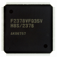
DF61657CN35FTV Renesas Electronics America, DF61657CN35FTV Datasheet - Page 89

DF61657CN35FTV
Manufacturer Part Number
DF61657CN35FTV
Description
IC H8SX/1657 MCU FLASH 120TQFP
Manufacturer
Renesas Electronics America
Series
H8® H8SX/1600r
Datasheet
1.DF61656N35FTV.pdf
(894 pages)
Specifications of DF61657CN35FTV
Core Processor
H8SX
Core Size
32-Bit
Speed
35MHz
Connectivity
SCI, SmartCard
Peripherals
DMA, PWM, WDT
Number Of I /o
82
Program Memory Size
768KB (768K x 8)
Program Memory Type
FLASH
Ram Size
24K x 8
Voltage - Supply (vcc/vdd)
3 V ~ 3.6 V
Data Converters
A/D 8x10b; D/A 2x8b
Oscillator Type
Internal
Operating Temperature
-20°C ~ 75°C
Package / Case
120-TQFP, 120-VQFP
For Use With
3DK1657 - DEV EVAL KIT FOR H8SX/1657
Lead Free Status / RoHS Status
Lead free / RoHS Compliant
Eeprom Size
-
Available stocks
Company
Part Number
Manufacturer
Quantity
Price
Company:
Part Number:
DF61657CN35FTV
Manufacturer:
RENESAS
Quantity:
101
Company:
Part Number:
DF61657CN35FTV
Manufacturer:
Renesas Electronics America
Quantity:
10 000
- Current page: 89 of 894
- Download datasheet (5Mb)
3.1
This LSI has seven operating modes (modes 1 to 7). The operating mode is selected by the setting
of mode pins (MD2 to MD0). Table 3.1 lists MCU operating mode settings.
Table 3.1
In this LSI, an advanced mode as the CPU operating mode and a 16-Mbyte address space are
available. The initial bus widths are eight or 16 bits. As the LSI initiation mode, the external
extended mode, on-chip ROM initiation mode single-chip initiation mode can be selected.
Modes 1 and 2 are the user boot mode and the boot mode in which the flash memory can be
programmed and erased. For details on the user boot mode and the boot mode, refer to section 18,
Flash Memory (0.18-µm F-ZTAT Version).
Mode 7 is a single-chip mode. All I/O ports can be used as general input/output ports. The external
address space cannot be accessed in the initial state, but setting the EXPE bit in the system control
register (SYSCR) to 1 enables the external address space. After the external address space is
enabled, ports D, E, and F can be used as an address output bus and ports H and I as a data bus by
specifying the data direction register (DDR) for each port.
MCU
Operating
Mode
1
2
3
4
5
6
7
Operating Mode Selection
0
0
0
1
1
1
1
MD2
MCU Operating Mode Settings
MD1
0
1
1
0
0
1
1
Section 3 MCU Operating Modes
MD0
1
0
1
0
1
0
1
CPU
Operating
Mode
Advanced
Advanced
Address
Space
16 Mbytes User boot mode
16 Mbytes
Reserved (setting prohibited)
LSI Initiation
Mode
Boot mode
On-chip ROM
disabled extended
mode
On-chip ROM
enabled extended
mode
Single-chip mode
Rev. 2.00 Jun. 28, 2007 Page 63 of 864
Section 3 MCU Operating Modes
On-Chip
ROM
Enabled
Enabled
Disabled
Disabled
Enabled
Enabled
REJ09B0341-0200
Default Max.
16 bits
8 bits
8 bits
External Data
Bus Width
16 bits
16 bits
16 bits
16 bits
16 bits
16 bits
Related parts for DF61657CN35FTV
Image
Part Number
Description
Manufacturer
Datasheet
Request
R

Part Number:
Description:
KIT STARTER FOR M16C/29
Manufacturer:
Renesas Electronics America
Datasheet:

Part Number:
Description:
KIT STARTER FOR R8C/2D
Manufacturer:
Renesas Electronics America
Datasheet:

Part Number:
Description:
R0K33062P STARTER KIT
Manufacturer:
Renesas Electronics America
Datasheet:

Part Number:
Description:
KIT STARTER FOR R8C/23 E8A
Manufacturer:
Renesas Electronics America
Datasheet:

Part Number:
Description:
KIT STARTER FOR R8C/25
Manufacturer:
Renesas Electronics America
Datasheet:

Part Number:
Description:
KIT STARTER H8S2456 SHARPE DSPLY
Manufacturer:
Renesas Electronics America
Datasheet:

Part Number:
Description:
KIT STARTER FOR R8C38C
Manufacturer:
Renesas Electronics America
Datasheet:

Part Number:
Description:
KIT STARTER FOR R8C35C
Manufacturer:
Renesas Electronics America
Datasheet:

Part Number:
Description:
KIT STARTER FOR R8CL3AC+LCD APPS
Manufacturer:
Renesas Electronics America
Datasheet:

Part Number:
Description:
KIT STARTER FOR RX610
Manufacturer:
Renesas Electronics America
Datasheet:

Part Number:
Description:
KIT STARTER FOR R32C/118
Manufacturer:
Renesas Electronics America
Datasheet:

Part Number:
Description:
KIT DEV RSK-R8C/26-29
Manufacturer:
Renesas Electronics America
Datasheet:

Part Number:
Description:
KIT STARTER FOR SH7124
Manufacturer:
Renesas Electronics America
Datasheet:

Part Number:
Description:
KIT STARTER FOR H8SX/1622
Manufacturer:
Renesas Electronics America
Datasheet:

Part Number:
Description:
KIT DEV FOR SH7203
Manufacturer:
Renesas Electronics America
Datasheet:


