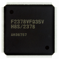
DF61657CN35FTV Renesas Electronics America, DF61657CN35FTV Datasheet - Page 193

DF61657CN35FTV
Manufacturer Part Number
DF61657CN35FTV
Description
IC H8SX/1657 MCU FLASH 120TQFP
Manufacturer
Renesas Electronics America
Series
H8® H8SX/1600r
Datasheet
1.DF61656N35FTV.pdf
(894 pages)
Specifications of DF61657CN35FTV
Core Processor
H8SX
Core Size
32-Bit
Speed
35MHz
Connectivity
SCI, SmartCard
Peripherals
DMA, PWM, WDT
Number Of I /o
82
Program Memory Size
768KB (768K x 8)
Program Memory Type
FLASH
Ram Size
24K x 8
Voltage - Supply (vcc/vdd)
3 V ~ 3.6 V
Data Converters
A/D 8x10b; D/A 2x8b
Oscillator Type
Internal
Operating Temperature
-20°C ~ 75°C
Package / Case
120-TQFP, 120-VQFP
For Use With
3DK1657 - DEV EVAL KIT FOR H8SX/1657
Lead Free Status / RoHS Status
Lead free / RoHS Compliant
Eeprom Size
-
Available stocks
Company
Part Number
Manufacturer
Quantity
Price
Company:
Part Number:
DF61657CN35FTV
Manufacturer:
RENESAS
Quantity:
101
Company:
Part Number:
DF61657CN35FTV
Manufacturer:
Renesas Electronics America
Quantity:
10 000
- Current page: 193 of 894
- Download datasheet (5Mb)
6.5.5
(1)
Area 0 includes on-chip ROM*. All of area 0 is used as external address space in on-chip ROM
disabled extended mode, and the space excluding on-chip ROM is external address space in on-
chip ROM enabled extended mode.
When area 0 external address space is accessed, the CS0 signal can be output.
Either of the basic bus interface, byte control SRAM interface, or burst ROM interface can be
selected for area 0 by bit BSRM0 in BROMCR and bit BCSEL0 in SRAMCR. Table 6.7 shows
the external interface of area 0.
Note: Applied to the LSI version that incorporates the ROM.
Table 6.7
(2)
In externally extended mode, all of area 1 is external address space. In on-chip ROM enabled
extended mode, the space excluding on-chip ROM* is external address space.
When area 1 external address space is accessed, the CS1 signal can be output.
Either of the basic bus interface, byte control SRAM, or burst ROM interface can be selected for
area 1 by bit BSRM1 in BROMCR and bit BCSEL1 in SRAMCR. Table 6.8 shows the external
interface of area 1.
Note: Applied to the LSI version that incorporates the ROM.
Interface
Basic bus interface
Byte control SRAM interface
Burst ROM interface
Setting prohibited
Area 0
Area 1
Area and External Bus Interface
Area 0 External Interface
BSRM0 of BROMCR
0
0
1
1
Register Setting
Rev. 2.00 Jun. 28, 2007 Page 167 of 864
BCSEL0 of SRAMCR
0
1
0
1
Section 6 Bus Controller (BSC)
REJ09B0341-0200
Related parts for DF61657CN35FTV
Image
Part Number
Description
Manufacturer
Datasheet
Request
R

Part Number:
Description:
KIT STARTER FOR M16C/29
Manufacturer:
Renesas Electronics America
Datasheet:

Part Number:
Description:
KIT STARTER FOR R8C/2D
Manufacturer:
Renesas Electronics America
Datasheet:

Part Number:
Description:
R0K33062P STARTER KIT
Manufacturer:
Renesas Electronics America
Datasheet:

Part Number:
Description:
KIT STARTER FOR R8C/23 E8A
Manufacturer:
Renesas Electronics America
Datasheet:

Part Number:
Description:
KIT STARTER FOR R8C/25
Manufacturer:
Renesas Electronics America
Datasheet:

Part Number:
Description:
KIT STARTER H8S2456 SHARPE DSPLY
Manufacturer:
Renesas Electronics America
Datasheet:

Part Number:
Description:
KIT STARTER FOR R8C38C
Manufacturer:
Renesas Electronics America
Datasheet:

Part Number:
Description:
KIT STARTER FOR R8C35C
Manufacturer:
Renesas Electronics America
Datasheet:

Part Number:
Description:
KIT STARTER FOR R8CL3AC+LCD APPS
Manufacturer:
Renesas Electronics America
Datasheet:

Part Number:
Description:
KIT STARTER FOR RX610
Manufacturer:
Renesas Electronics America
Datasheet:

Part Number:
Description:
KIT STARTER FOR R32C/118
Manufacturer:
Renesas Electronics America
Datasheet:

Part Number:
Description:
KIT DEV RSK-R8C/26-29
Manufacturer:
Renesas Electronics America
Datasheet:

Part Number:
Description:
KIT STARTER FOR SH7124
Manufacturer:
Renesas Electronics America
Datasheet:

Part Number:
Description:
KIT STARTER FOR H8SX/1622
Manufacturer:
Renesas Electronics America
Datasheet:

Part Number:
Description:
KIT DEV FOR SH7203
Manufacturer:
Renesas Electronics America
Datasheet:


