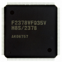
DF61657CN35FTV Renesas Electronics America, DF61657CN35FTV Datasheet - Page 590

DF61657CN35FTV
Manufacturer Part Number
DF61657CN35FTV
Description
IC H8SX/1657 MCU FLASH 120TQFP
Manufacturer
Renesas Electronics America
Series
H8® H8SX/1600r
Datasheet
1.DF61656N35FTV.pdf
(894 pages)
Specifications of DF61657CN35FTV
Core Processor
H8SX
Core Size
32-Bit
Speed
35MHz
Connectivity
SCI, SmartCard
Peripherals
DMA, PWM, WDT
Number Of I /o
82
Program Memory Size
768KB (768K x 8)
Program Memory Type
FLASH
Ram Size
24K x 8
Voltage - Supply (vcc/vdd)
3 V ~ 3.6 V
Data Converters
A/D 8x10b; D/A 2x8b
Oscillator Type
Internal
Operating Temperature
-20°C ~ 75°C
Package / Case
120-TQFP, 120-VQFP
For Use With
3DK1657 - DEV EVAL KIT FOR H8SX/1657
Lead Free Status / RoHS Status
Lead free / RoHS Compliant
Eeprom Size
-
Available stocks
Company
Part Number
Manufacturer
Quantity
Price
Company:
Part Number:
DF61657CN35FTV
Manufacturer:
RENESAS
Quantity:
101
Company:
Part Number:
DF61657CN35FTV
Manufacturer:
Renesas Electronics America
Quantity:
10 000
- Current page: 590 of 894
- Download datasheet (5Mb)
Section 14 Serial Communication Interface (SCI)
14.3.7
SSR is a register containing status flags of the SCI and multiprocessor bits for transfer. TDRE,
RDRF, ORER, PER, and FER can only be cleared. Some bits in SSR have different functions in
normal mode and smart card interface mode.
• When SMIF in SCMR = 0
• When SMIF in SCMR = 1
Rev. 2.00 Jun. 28, 2007 Page 564 of 864
REJ09B0341-0200
Bit
1
0
Bit
Bit Name
Initial Value
R/W
Bit
Bit Name
Initial Value
R/W
Note: * Only 0 can be written, to clear the flag.
Note: * Only 0 can be written, to clear the flag.
Bit Name
CKE1
CKE0
Serial Status Register (SSR)
R/(W)*
R/(W)*
TDRE
TDRE
7
1
7
1
Initial
Value
0
0
R/(W)*
R/(W)*
RDRF
RDRF
6
0
6
0
R/W
R/W
R/W
R/(W)*
ORER
R/(W)*
ORER
5
0
5
0
Description
Clock Enable 1, 0
These bits control the clock output from the SCK pin. In
GSM mode, clock output can be dynamically switched.
For details, see section 14.7.8, Clock Output Control.
•
00: Output disabled (SCK pin functions as I/O port.)
01: Clock output
1X: Reserved
•
00: Output fixed low
01: Clock output
10: Output fixed high
11: Clock output
When GM in SMR = 0
When GM in SMR = 1
R/(W)*
R/(W)*
FRE
ERS
4
0
4
0
R/(W)*
R/(W)*
PER
PER
3
0
3
0
TEND
TEND
R
2
1
R
2
1
MPB
MPB
R
1
0
R
1
0
MPBT
MPBT
R/W
R/W
0
0
0
0
Related parts for DF61657CN35FTV
Image
Part Number
Description
Manufacturer
Datasheet
Request
R

Part Number:
Description:
KIT STARTER FOR M16C/29
Manufacturer:
Renesas Electronics America
Datasheet:

Part Number:
Description:
KIT STARTER FOR R8C/2D
Manufacturer:
Renesas Electronics America
Datasheet:

Part Number:
Description:
R0K33062P STARTER KIT
Manufacturer:
Renesas Electronics America
Datasheet:

Part Number:
Description:
KIT STARTER FOR R8C/23 E8A
Manufacturer:
Renesas Electronics America
Datasheet:

Part Number:
Description:
KIT STARTER FOR R8C/25
Manufacturer:
Renesas Electronics America
Datasheet:

Part Number:
Description:
KIT STARTER H8S2456 SHARPE DSPLY
Manufacturer:
Renesas Electronics America
Datasheet:

Part Number:
Description:
KIT STARTER FOR R8C38C
Manufacturer:
Renesas Electronics America
Datasheet:

Part Number:
Description:
KIT STARTER FOR R8C35C
Manufacturer:
Renesas Electronics America
Datasheet:

Part Number:
Description:
KIT STARTER FOR R8CL3AC+LCD APPS
Manufacturer:
Renesas Electronics America
Datasheet:

Part Number:
Description:
KIT STARTER FOR RX610
Manufacturer:
Renesas Electronics America
Datasheet:

Part Number:
Description:
KIT STARTER FOR R32C/118
Manufacturer:
Renesas Electronics America
Datasheet:

Part Number:
Description:
KIT DEV RSK-R8C/26-29
Manufacturer:
Renesas Electronics America
Datasheet:

Part Number:
Description:
KIT STARTER FOR SH7124
Manufacturer:
Renesas Electronics America
Datasheet:

Part Number:
Description:
KIT STARTER FOR H8SX/1622
Manufacturer:
Renesas Electronics America
Datasheet:

Part Number:
Description:
KIT DEV FOR SH7203
Manufacturer:
Renesas Electronics America
Datasheet:


