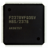
DF61657CN35FTV Renesas Electronics America, DF61657CN35FTV Datasheet - Page 523

DF61657CN35FTV
Manufacturer Part Number
DF61657CN35FTV
Description
IC H8SX/1657 MCU FLASH 120TQFP
Manufacturer
Renesas Electronics America
Series
H8® H8SX/1600r
Datasheet
1.DF61656N35FTV.pdf
(894 pages)
Specifications of DF61657CN35FTV
Core Processor
H8SX
Core Size
32-Bit
Speed
35MHz
Connectivity
SCI, SmartCard
Peripherals
DMA, PWM, WDT
Number Of I /o
82
Program Memory Size
768KB (768K x 8)
Program Memory Type
FLASH
Ram Size
24K x 8
Voltage - Supply (vcc/vdd)
3 V ~ 3.6 V
Data Converters
A/D 8x10b; D/A 2x8b
Oscillator Type
Internal
Operating Temperature
-20°C ~ 75°C
Package / Case
120-TQFP, 120-VQFP
For Use With
3DK1657 - DEV EVAL KIT FOR H8SX/1657
Lead Free Status / RoHS Status
Lead free / RoHS Compliant
Eeprom Size
-
Available stocks
Company
Part Number
Manufacturer
Quantity
Price
Company:
Part Number:
DF61657CN35FTV
Manufacturer:
RENESAS
Quantity:
101
Company:
Part Number:
DF61657CN35FTV
Manufacturer:
Renesas Electronics America
Quantity:
10 000
- Current page: 523 of 894
- Download datasheet (5Mb)
• NDRH
Bit
7
6
5
4
3
2
1
0
Bit
7
6
5
4
3 to 0
Bit
7 to 4
3
2
1
0
If pulse output groups 2 and 3 have the same output trigger, all eight bits are mapped to the
same address and can be accessed at one time, as shown below.
If pulse output groups 2 and 3 have different output triggers, the upper four bits and lower four
bits are mapped to different addresses as shown below.
Bit Name
NDR15
NDR14
NDR13
NDR12
NDR11
NDR10
NDR9
NDR8
Bit Name
NDR15
NDR14
NDR13
NDR12
Bit Name
NDR11
NDR10
NDR9
NDR8
Initial
Value
0
0
0
0
0
0
0
0
Initial
Value
0
0
0
0
All 1
Initial
Value
All 1
0
0
0
0
R/W
R/W
R/W
R/W
R/W
R/W
R/W
R/W
R/W
R/W
R/W
R/W
R/W
R/W
R/W
R/W
R/W
R/W
R/W
Description
Next Data Register 15 to 8
The register contents are transferred to the
corresponding PODRH bits by the output trigger specified
with PCR.
Description
Next Data Register 15 to 12
The register contents are transferred to the
corresponding PODRH bits by the output trigger specified
with PCR.
Reserved
These bits are always read as 1 and cannot be modified.
Description
Reserved
These bits are always read as 1 and cannot be modified.
Next Data Register 11 to 8
The register contents are transferred to the
corresponding PODRH bits by the output trigger specified
with PCR.
Section 11 Programmable Pulse Generator (PPG)
Rev. 2.00 Jun. 28, 2007 Page 497 of 864
REJ09B0341-0200
Related parts for DF61657CN35FTV
Image
Part Number
Description
Manufacturer
Datasheet
Request
R

Part Number:
Description:
KIT STARTER FOR M16C/29
Manufacturer:
Renesas Electronics America
Datasheet:

Part Number:
Description:
KIT STARTER FOR R8C/2D
Manufacturer:
Renesas Electronics America
Datasheet:

Part Number:
Description:
R0K33062P STARTER KIT
Manufacturer:
Renesas Electronics America
Datasheet:

Part Number:
Description:
KIT STARTER FOR R8C/23 E8A
Manufacturer:
Renesas Electronics America
Datasheet:

Part Number:
Description:
KIT STARTER FOR R8C/25
Manufacturer:
Renesas Electronics America
Datasheet:

Part Number:
Description:
KIT STARTER H8S2456 SHARPE DSPLY
Manufacturer:
Renesas Electronics America
Datasheet:

Part Number:
Description:
KIT STARTER FOR R8C38C
Manufacturer:
Renesas Electronics America
Datasheet:

Part Number:
Description:
KIT STARTER FOR R8C35C
Manufacturer:
Renesas Electronics America
Datasheet:

Part Number:
Description:
KIT STARTER FOR R8CL3AC+LCD APPS
Manufacturer:
Renesas Electronics America
Datasheet:

Part Number:
Description:
KIT STARTER FOR RX610
Manufacturer:
Renesas Electronics America
Datasheet:

Part Number:
Description:
KIT STARTER FOR R32C/118
Manufacturer:
Renesas Electronics America
Datasheet:

Part Number:
Description:
KIT DEV RSK-R8C/26-29
Manufacturer:
Renesas Electronics America
Datasheet:

Part Number:
Description:
KIT STARTER FOR SH7124
Manufacturer:
Renesas Electronics America
Datasheet:

Part Number:
Description:
KIT STARTER FOR H8SX/1622
Manufacturer:
Renesas Electronics America
Datasheet:

Part Number:
Description:
KIT DEV FOR SH7203
Manufacturer:
Renesas Electronics America
Datasheet:


