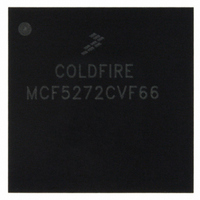
MCF5272CVF66 Freescale Semiconductor, MCF5272CVF66 Datasheet - Page 308

MCF5272CVF66
Manufacturer Part Number
MCF5272CVF66
Description
IC MPU 32BIT 66MHZ 196-MAPBGA
Manufacturer
Freescale Semiconductor
Series
MCF527xr
Specifications of MCF5272CVF66
Core Processor
Coldfire V2
Core Size
32-Bit
Speed
66MHz
Connectivity
EBI/EMI, Ethernet, I²C, SPI, UART/USART, USB
Peripherals
DMA, WDT
Number Of I /o
32
Program Memory Size
16KB (4K x 32)
Program Memory Type
ROM
Ram Size
1K x 32
Voltage - Supply (vcc/vdd)
3 V ~ 3.6 V
Oscillator Type
External
Operating Temperature
-40°C ~ 85°C
Package / Case
196-MAPBGA
Family Name
MCF5xxx
Device Core
ColdFire
Device Core Size
32b
Frequency (max)
66MHz
Instruction Set Architecture
RISC
Supply Voltage 1 (typ)
3.3V
Operating Temp Range
-40C to 85C
Operating Temperature Classification
Industrial
Mounting
Surface Mount
Pin Count
196
Package Type
MA-BGA
Lead Free Status / RoHS Status
Contains lead / RoHS non-compliant
Eeprom Size
-
Data Converters
-
Lead Free Status / Rohs Status
Not Compliant
Available stocks
Company
Part Number
Manufacturer
Quantity
Price
Company:
Part Number:
MCF5272CVF66
Manufacturer:
Freescale Semiconductor
Quantity:
10 000
Part Number:
MCF5272CVF66
Manufacturer:
FREESCALE
Quantity:
20 000
Company:
Part Number:
MCF5272CVF66 K75N
Manufacturer:
ST
Quantity:
18
Company:
Part Number:
MCF5272CVF66J
Manufacturer:
Freescale Semiconductor
Quantity:
10 000
- Current page: 308 of 544
- Download datasheet (7Mb)
Physical Layer Interface Controller (PLIC)
The above settings can be made by a single write of the 16-bit value 0x802B to PCSR.
The following restrictions should be observed when using the clock generator module:
Figure 13-11
PLIC block.
13-12
•
•
The smallest multiplication factor is 2.
CLKIN should be significantly greater than (> 20 times) the synthesized clock.
DCL0/URT1_CLK
PA8/FSC0/FSR0
GCI/IDL
GCI/IDL
GCI/IDL
GCI/IDL
Port 1
Port 2
Port 3
Port 0
and
O192K
P1CR[FSM]
Figure 13-12
FSC0
FSC1
MCF5272 ColdFire
DCL0
DFSC0
DCL1
FSC1
DCL1
DFSC2
DCL1
DFSC3
CKI[1:0]
Mux
Figure 13-11. PLIC Internal Timing Signal Routing
show the connectivity and relationship of the timing signals within the
DFSC0
Figure 13-12. PLIC Clock Generator
®
Prog Delay 0
Integrated Microprocessor User’s Manual, Rev. 3
P0SDR[15:0]
P1SDR[15:0]
P2SDR[15:0]
P3SDR[15:0]
CMULT[2:0]
Multiply
Prog Delay 1
Prog Delay 2
Block
Prog Delay 3
SFSC Gen
P0CR[M2-M0]
DFSC1
P1CR[M/S]
Pin
Mux 1
Pin
Mux 0
2-KHz to CPU
FDIV[2:0]
Divider
Block
DCL0/URT1_CLK
PA8/FSC0/FSR0
DCL1/GDCL1_OUT
FSC1/FSR1/DFSC1
DFSC2
DFSC3
Freescale Semiconductor
GDCL
Gen_FSC
Related parts for MCF5272CVF66
Image
Part Number
Description
Manufacturer
Datasheet
Request
R
Part Number:
Description:
Mcf5272 Coldfire Integrated Microprocessor User
Manufacturer:
Freescale Semiconductor, Inc
Datasheet:

Part Number:
Description:
MCF5272 Interrupt Service Routine for the Physical Layer Interface Controller
Manufacturer:
Freescale Semiconductor / Motorola
Datasheet:
Part Number:
Description:
Manufacturer:
Freescale Semiconductor, Inc
Datasheet:
Part Number:
Description:
Manufacturer:
Freescale Semiconductor, Inc
Datasheet:
Part Number:
Description:
Manufacturer:
Freescale Semiconductor, Inc
Datasheet:
Part Number:
Description:
Manufacturer:
Freescale Semiconductor, Inc
Datasheet:
Part Number:
Description:
Manufacturer:
Freescale Semiconductor, Inc
Datasheet:
Part Number:
Description:
Manufacturer:
Freescale Semiconductor, Inc
Datasheet:
Part Number:
Description:
Manufacturer:
Freescale Semiconductor, Inc
Datasheet:
Part Number:
Description:
Manufacturer:
Freescale Semiconductor, Inc
Datasheet:
Part Number:
Description:
Manufacturer:
Freescale Semiconductor, Inc
Datasheet:
Part Number:
Description:
Manufacturer:
Freescale Semiconductor, Inc
Datasheet:
Part Number:
Description:
Manufacturer:
Freescale Semiconductor, Inc
Datasheet:
Part Number:
Description:
Manufacturer:
Freescale Semiconductor, Inc
Datasheet:
Part Number:
Description:
Manufacturer:
Freescale Semiconductor, Inc
Datasheet:


