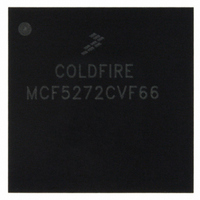
MCF5272CVF66 Freescale Semiconductor, MCF5272CVF66 Datasheet - Page 476

MCF5272CVF66
Manufacturer Part Number
MCF5272CVF66
Description
IC MPU 32BIT 66MHZ 196-MAPBGA
Manufacturer
Freescale Semiconductor
Series
MCF527xr
Specifications of MCF5272CVF66
Core Processor
Coldfire V2
Core Size
32-Bit
Speed
66MHz
Connectivity
EBI/EMI, Ethernet, I²C, SPI, UART/USART, USB
Peripherals
DMA, WDT
Number Of I /o
32
Program Memory Size
16KB (4K x 32)
Program Memory Type
ROM
Ram Size
1K x 32
Voltage - Supply (vcc/vdd)
3 V ~ 3.6 V
Oscillator Type
External
Operating Temperature
-40°C ~ 85°C
Package / Case
196-MAPBGA
Family Name
MCF5xxx
Device Core
ColdFire
Device Core Size
32b
Frequency (max)
66MHz
Instruction Set Architecture
RISC
Supply Voltage 1 (typ)
3.3V
Operating Temp Range
-40C to 85C
Operating Temperature Classification
Industrial
Mounting
Surface Mount
Pin Count
196
Package Type
MA-BGA
Lead Free Status / RoHS Status
Contains lead / RoHS non-compliant
Eeprom Size
-
Data Converters
-
Lead Free Status / Rohs Status
Not Compliant
Available stocks
Company
Part Number
Manufacturer
Quantity
Price
Company:
Part Number:
MCF5272CVF66
Manufacturer:
Freescale Semiconductor
Quantity:
10 000
Part Number:
MCF5272CVF66
Manufacturer:
FREESCALE
Quantity:
20 000
Company:
Part Number:
MCF5272CVF66 K75N
Manufacturer:
ST
Quantity:
18
Company:
Part Number:
MCF5272CVF66J
Manufacturer:
Freescale Semiconductor
Quantity:
10 000
- Current page: 476 of 544
- Download datasheet (7Mb)
IEEE 1149.1 Test Access Port (JTAG)
Figure 21-1
21.2
The JTAG test interface shares pins with the debug modules (see
21-2
PSTCLK
Signal
BKPT
TMS/
TDO/
TCK/
DSO
TMS
TCK
TDI
JTAG Test Access Port and BDM Debug Port
Test clock. TCK is the dedicated JTAG test logic clock input, independent of the CPU system clock. It provides a
clock for on-board test logic defined by the IEEE 1149.1 standard. TCK should be grounded if the JTAG port is not
used and MTMOD is tied low.
Test mode select. This input controls test mode operations for on-board test logic defined by the IEEE 1149.1
standard. Connecting TMS to VDD disables the test controller, making all JTAG circuits transparent to the system.
Test and debug data out. Output for shifting data out of serial data port logic. Shifting out data depends on the state
of the JTAG controller state machine and the instructions in the instruction register. The shift occurs on the falling
edge of TCK. When not outputting data, TDO is placed in high-impedance state. TDO can also be three-stated to
allow bused or parallel connections to other devices having JTAG test access ports.
shows the MCF5272 implementation of IEEE 1149.1.
Precautions to ensure that the IEEE 1149.1 test logic does not interfere with
non-test operation are described in
Operation.”
Controller
TAP
MCF5272 ColdFire
3
4-Bit Instruction Register
Figure 21-1. Test Access Port Block Diagram
Boundary-Scan Register
Decoder
Test Data Register
®
Integrated Microprocessor User’s Manual, Rev. 3
Table 21-1. JTAG Signals
ID (32 bits)
Bypass
0
(1 Bit)
NOTE
Section 21.7, “Non-IEEE 1149.1
Description
Table
21-1).
Freescale Semiconductor
TDC
Related parts for MCF5272CVF66
Image
Part Number
Description
Manufacturer
Datasheet
Request
R
Part Number:
Description:
Mcf5272 Coldfire Integrated Microprocessor User
Manufacturer:
Freescale Semiconductor, Inc
Datasheet:

Part Number:
Description:
MCF5272 Interrupt Service Routine for the Physical Layer Interface Controller
Manufacturer:
Freescale Semiconductor / Motorola
Datasheet:
Part Number:
Description:
Manufacturer:
Freescale Semiconductor, Inc
Datasheet:
Part Number:
Description:
Manufacturer:
Freescale Semiconductor, Inc
Datasheet:
Part Number:
Description:
Manufacturer:
Freescale Semiconductor, Inc
Datasheet:
Part Number:
Description:
Manufacturer:
Freescale Semiconductor, Inc
Datasheet:
Part Number:
Description:
Manufacturer:
Freescale Semiconductor, Inc
Datasheet:
Part Number:
Description:
Manufacturer:
Freescale Semiconductor, Inc
Datasheet:
Part Number:
Description:
Manufacturer:
Freescale Semiconductor, Inc
Datasheet:
Part Number:
Description:
Manufacturer:
Freescale Semiconductor, Inc
Datasheet:
Part Number:
Description:
Manufacturer:
Freescale Semiconductor, Inc
Datasheet:
Part Number:
Description:
Manufacturer:
Freescale Semiconductor, Inc
Datasheet:
Part Number:
Description:
Manufacturer:
Freescale Semiconductor, Inc
Datasheet:
Part Number:
Description:
Manufacturer:
Freescale Semiconductor, Inc
Datasheet:
Part Number:
Description:
Manufacturer:
Freescale Semiconductor, Inc
Datasheet:


