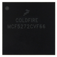
MCF5272CVF66 Freescale Semiconductor, MCF5272CVF66 Datasheet - Page 470

MCF5272CVF66
Manufacturer Part Number
MCF5272CVF66
Description
IC MPU 32BIT 66MHZ 196-MAPBGA
Manufacturer
Freescale Semiconductor
Series
MCF527xr
Specifications of MCF5272CVF66
Core Processor
Coldfire V2
Core Size
32-Bit
Speed
66MHz
Connectivity
EBI/EMI, Ethernet, I²C, SPI, UART/USART, USB
Peripherals
DMA, WDT
Number Of I /o
32
Program Memory Size
16KB (4K x 32)
Program Memory Type
ROM
Ram Size
1K x 32
Voltage - Supply (vcc/vdd)
3 V ~ 3.6 V
Oscillator Type
External
Operating Temperature
-40°C ~ 85°C
Package / Case
196-MAPBGA
Family Name
MCF5xxx
Device Core
ColdFire
Device Core Size
32b
Frequency (max)
66MHz
Instruction Set Architecture
RISC
Supply Voltage 1 (typ)
3.3V
Operating Temp Range
-40C to 85C
Operating Temperature Classification
Industrial
Mounting
Surface Mount
Pin Count
196
Package Type
MA-BGA
Lead Free Status / RoHS Status
Contains lead / RoHS non-compliant
Eeprom Size
-
Data Converters
-
Lead Free Status / Rohs Status
Not Compliant
Available stocks
Company
Part Number
Manufacturer
Quantity
Price
Company:
Part Number:
MCF5272CVF66
Manufacturer:
Freescale Semiconductor
Quantity:
10 000
Part Number:
MCF5272CVF66
Manufacturer:
FREESCALE
Quantity:
20 000
Company:
Part Number:
MCF5272CVF66 K75N
Manufacturer:
ST
Quantity:
18
Company:
Part Number:
MCF5272CVF66J
Manufacturer:
Freescale Semiconductor
Quantity:
10 000
- Current page: 470 of 544
- Download datasheet (7Mb)
Bus Operation
20.12.1 Master Reset
To perform a master reset, an external device asserts RSTI and DRESETEN simultaneously for a
minimum of six CLKIN cycles after VDD is within tolerance. This should always be done when power is
initially applied. A master reset resets the entire device including the SDRAM controller.
Figure 20-21
VDD, RSTI, DRESETEN, RSTO, mode selects, and bus signals.
CLKIN must be stable by the time VDD reaches the minimum operating specification. RSTI and
DRESETEN are internally synchronized on consecutive rising and falling clocks before being used. They
must meet the specified setup and hold times to the falling edge of CLKIN only if recognition by a specific
falling edge is required
When the assertion of RSTI is recognized internally, the MCF5272 asserts the reset out pin (RSTO). The
RSTO pin is asserted as long as RSTI is asserted and remains asserted for 32,768 CLKIN cycles after RSTI
is negated.
During the master reset period, all outputs are driven to their default levels. Once RSTO negates, all bus
signals continue to remain in this state until the ColdFire core begins the first bus cycle for reset exception
processing.
The levels of the mode select inputs, QSPI_Dout/WSEL, QSPI_CLK/BUSW1, and QSPI_CS0/BUSW0,
are sampled when RSTO negates and they select the port size of CS0 and the physical data bus width after
a master reset occurs. The INTx signals are synchronized and are registered on the last falling edge of
CLKIN where RSTI is asserted.
A master reset causes any bus cycle (including SDRAM refresh cycles) to terminate. In addition, master
reset initializes registers appropriately for a reset exception. During an external master reset,
SCR[RSTSRC] is set to 0b11 to indicate that assertion of RSTI and DRESETEN caused the previous reset.
20-22
.
CLKIN
VDD
RSTI
DRESETEN
Mode Select
Inputs
RSTO
BUS SIGNALS
is a functional timing diagram of the master reset operation, illustrating relationships among
MCF5272 ColdFire
Figure 20-21. Master Reset Timing
®
Integrated Microprocessor User’s Manual, Rev. 3
CLK CYCLES
T >= 6
CLK CYCLES
T = 32,768
CLK CYCLES
T >= 22
Freescale Semiconductor
Related parts for MCF5272CVF66
Image
Part Number
Description
Manufacturer
Datasheet
Request
R
Part Number:
Description:
Mcf5272 Coldfire Integrated Microprocessor User
Manufacturer:
Freescale Semiconductor, Inc
Datasheet:

Part Number:
Description:
MCF5272 Interrupt Service Routine for the Physical Layer Interface Controller
Manufacturer:
Freescale Semiconductor / Motorola
Datasheet:
Part Number:
Description:
Manufacturer:
Freescale Semiconductor, Inc
Datasheet:
Part Number:
Description:
Manufacturer:
Freescale Semiconductor, Inc
Datasheet:
Part Number:
Description:
Manufacturer:
Freescale Semiconductor, Inc
Datasheet:
Part Number:
Description:
Manufacturer:
Freescale Semiconductor, Inc
Datasheet:
Part Number:
Description:
Manufacturer:
Freescale Semiconductor, Inc
Datasheet:
Part Number:
Description:
Manufacturer:
Freescale Semiconductor, Inc
Datasheet:
Part Number:
Description:
Manufacturer:
Freescale Semiconductor, Inc
Datasheet:
Part Number:
Description:
Manufacturer:
Freescale Semiconductor, Inc
Datasheet:
Part Number:
Description:
Manufacturer:
Freescale Semiconductor, Inc
Datasheet:
Part Number:
Description:
Manufacturer:
Freescale Semiconductor, Inc
Datasheet:
Part Number:
Description:
Manufacturer:
Freescale Semiconductor, Inc
Datasheet:
Part Number:
Description:
Manufacturer:
Freescale Semiconductor, Inc
Datasheet:
Part Number:
Description:
Manufacturer:
Freescale Semiconductor, Inc
Datasheet:


