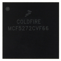
MCF5272CVF66 Freescale Semiconductor, MCF5272CVF66 Datasheet - Page 490

MCF5272CVF66
Manufacturer Part Number
MCF5272CVF66
Description
IC MPU 32BIT 66MHZ 196-MAPBGA
Manufacturer
Freescale Semiconductor
Series
MCF527xr
Specifications of MCF5272CVF66
Core Processor
Coldfire V2
Core Size
32-Bit
Speed
66MHz
Connectivity
EBI/EMI, Ethernet, I²C, SPI, UART/USART, USB
Peripherals
DMA, WDT
Number Of I /o
32
Program Memory Size
16KB (4K x 32)
Program Memory Type
ROM
Ram Size
1K x 32
Voltage - Supply (vcc/vdd)
3 V ~ 3.6 V
Oscillator Type
External
Operating Temperature
-40°C ~ 85°C
Package / Case
196-MAPBGA
Family Name
MCF5xxx
Device Core
ColdFire
Device Core Size
32b
Frequency (max)
66MHz
Instruction Set Architecture
RISC
Supply Voltage 1 (typ)
3.3V
Operating Temp Range
-40C to 85C
Operating Temperature Classification
Industrial
Mounting
Surface Mount
Pin Count
196
Package Type
MA-BGA
Lead Free Status / RoHS Status
Contains lead / RoHS non-compliant
Eeprom Size
-
Data Converters
-
Lead Free Status / Rohs Status
Not Compliant
Available stocks
Company
Part Number
Manufacturer
Quantity
Price
Company:
Part Number:
MCF5272CVF66
Manufacturer:
Freescale Semiconductor
Quantity:
10 000
Part Number:
MCF5272CVF66
Manufacturer:
FREESCALE
Quantity:
20 000
Company:
Part Number:
MCF5272CVF66 K75N
Manufacturer:
ST
Quantity:
18
Company:
Part Number:
MCF5272CVF66J
Manufacturer:
Freescale Semiconductor
Quantity:
10 000
- Current page: 490 of 544
- Download datasheet (7Mb)
Electrical Characteristics
23.3.2
Table 23-7
1
2
23-6
B1a
B1b
B1c
B1d
B1e
B1f
B2d
B2e
B2f
B3
B4
B5
Name
All timing references to SDCLK are given to its rising edge when bit 3 of the SDRAM control register is 0.
RSTI, TA, TEA, and INTx are synchronized internally. The setup time must be met only if recognition is needed on a particular
clock edge.
2
2
2
2
2
RSTI valid to SDCLK (setup)
TA valid to SDCLK (setup)
TEA valid to SDCLK (setup)
INTx valid to SDCLK (setup)
BKPT valid to PSTCLK (setup)
Mode selects (BUSW[1:0], WSEL, HiZ) valid to SDCLK (setup) (when RSTI asserted)
SDCLK to asynchronous control inputs (RSTI, TA, TEA, INTx) invalid (hold)
SDCLK to mode selects (BUSW[1,0], WSEL, HIZ) invalid (hold) (when RSTI asserted)
PSTCLK to asynchronous control input BKPT invalid (hold)
RSTI width low
Data input (D[31:0]) valid to SDCLK (setup)
SDCLK to data input (D[31:0]) invalid (hold)
lists processor bus input timings.
Processor Bus Input Timing Specifications
All processor bus timings are synchronous; that is, input setup/hold and
output delay with respect to the rising edge of a reference clock. The
reference clock is the SDCLK output.
All other timing relationships can be derived from these values.
MCF5272 ColdFire
Table 23-7. Processor Bus Input Timing Specifications
®
Integrated Microprocessor User’s Manual, Rev. 3
Characteristic
Control Inputs
Data Inputs
NOTE
1
Freescale Semiconductor
Min
10T
0–66 MHz
6.5
10
14
8
8
8
8
2
2
0
0
Max
—
—
—
—
—
—
—
—
—
—
—
—
Unit
nS
nS
nS
nS
nS
nS
nS
nS
nS
nS
nS
nS
Related parts for MCF5272CVF66
Image
Part Number
Description
Manufacturer
Datasheet
Request
R
Part Number:
Description:
Mcf5272 Coldfire Integrated Microprocessor User
Manufacturer:
Freescale Semiconductor, Inc
Datasheet:

Part Number:
Description:
MCF5272 Interrupt Service Routine for the Physical Layer Interface Controller
Manufacturer:
Freescale Semiconductor / Motorola
Datasheet:
Part Number:
Description:
Manufacturer:
Freescale Semiconductor, Inc
Datasheet:
Part Number:
Description:
Manufacturer:
Freescale Semiconductor, Inc
Datasheet:
Part Number:
Description:
Manufacturer:
Freescale Semiconductor, Inc
Datasheet:
Part Number:
Description:
Manufacturer:
Freescale Semiconductor, Inc
Datasheet:
Part Number:
Description:
Manufacturer:
Freescale Semiconductor, Inc
Datasheet:
Part Number:
Description:
Manufacturer:
Freescale Semiconductor, Inc
Datasheet:
Part Number:
Description:
Manufacturer:
Freescale Semiconductor, Inc
Datasheet:
Part Number:
Description:
Manufacturer:
Freescale Semiconductor, Inc
Datasheet:
Part Number:
Description:
Manufacturer:
Freescale Semiconductor, Inc
Datasheet:
Part Number:
Description:
Manufacturer:
Freescale Semiconductor, Inc
Datasheet:
Part Number:
Description:
Manufacturer:
Freescale Semiconductor, Inc
Datasheet:
Part Number:
Description:
Manufacturer:
Freescale Semiconductor, Inc
Datasheet:
Part Number:
Description:
Manufacturer:
Freescale Semiconductor, Inc
Datasheet:


