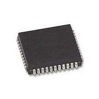
XR88C681J-F Exar Corporation, XR88C681J-F Datasheet - Page 54

XR88C681J-F
Manufacturer Part Number
XR88C681J-F
Description
IC UART CMOS DUAL 44PLCC
Manufacturer
Exar Corporation
Type
CMOS Dual Channel UARTr
Datasheet
1.XR88C681CP40-F.pdf
(101 pages)
Specifications of XR88C681J-F
Number Of Channels
2, DUART
Package / Case
44-LCC (J-Lead)
Features
*
Fifo's
1 Byte, 3 Byte
Voltage - Supply
5V
With Parallel Port
Yes
With Cmos
Yes
Mounting Type
Surface Mount
Data Rate
1 Mbps
Supply Voltage (max)
5.25 V
Supply Voltage (min)
4.75 V
Supply Current
15 mA
Maximum Operating Temperature
+ 85 C
Minimum Operating Temperature
- 40 C
Mounting Style
SMD/SMT
Operating Supply Voltage
5 V
Propagation Delay Time Ns
400 ns
No. Of Channels
2
Supply Voltage Range
4.75V To 5.25V
Operating Temperature Range
-40°C To +85°C
Digital Ic Case Style
PLCC
No. Of Pins
44
Filter Terminals
SMD
Rohs Compliant
Yes
Lead Free Status / RoHS Status
Lead free / RoHS Compliant
Lead Free Status / RoHS Status
Lead free / RoHS Compliant, Lead free / RoHS Compliant
Other names
1016-1329
Available stocks
Company
Part Number
Manufacturer
Quantity
Price
Company:
Part Number:
XR88C681J-F
Manufacturer:
Exar Corporation
Quantity:
10 000
D.3 Counter/Timer
The Timing Control Block also contains a 16 bit
Counter/Timer (C/T). The C/T is a programmable 16 bit
down-counter which can use one of several timing
sources as its input. Figure 28 presents a block diagram
of the circuitry surrounding the C/T. The selection of these
Bit 6
Rev. 2.11
0
0
0
0
1
1
1
1
Bit 5
0
0
1
1
0
0
1
1
Oscillator
Circuit
TXCB
TXCA
IP2
Figure 28. A Block Diagram of the Circuitry Associated with the
Bit 4
0
1
0
1
0
1
0
1
Divide by 16
Divide by 16
Table 16. ACR[6:4] Bit Field Definition - C/T
C/T Mode
Counter
Counter
Counter
Counter
Timer
Timer
Timer
Timer
Counter/Timer
Preset Registers
(CTUR, CTLR)
Counter/Timer
54
ACR[4-6]
timing sources for the Counter/Timer can be made by
writing the appropriate data to ACR[6:4] (Auxiliary Control
Register bits 6 through 4). Please see Table 16 for the
relationship between the Counter/Timer mode, the
Timing Source and ACR[6:4]. The C/T output is available
to the Clock Select Registers for use as a programmable
bit rate generator for both Transmitters and Receivers.
Timing Source
External Input - IP2
TXCA 1X - Clock of Channel A Transmitter
TXCB 1X - Clock of Channel B Transmitter
X1/CLK Input Divided by 16
External Input - IP2
External Input - IP2, Divided by 16
X1/CLK Input
X1/CLK Input Divided by 16
C/T_RDY
to 32:1 MUXs
(OP3)


