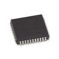
XR88C681J-F Exar Corporation, XR88C681J-F Datasheet - Page 67

XR88C681J-F
Manufacturer Part Number
XR88C681J-F
Description
IC UART CMOS DUAL 44PLCC
Manufacturer
Exar Corporation
Type
CMOS Dual Channel UARTr
Datasheet
1.XR88C681CP40-F.pdf
(101 pages)
Specifications of XR88C681J-F
Number Of Channels
2, DUART
Package / Case
44-LCC (J-Lead)
Features
*
Fifo's
1 Byte, 3 Byte
Voltage - Supply
5V
With Parallel Port
Yes
With Cmos
Yes
Mounting Type
Surface Mount
Data Rate
1 Mbps
Supply Voltage (max)
5.25 V
Supply Voltage (min)
4.75 V
Supply Current
15 mA
Maximum Operating Temperature
+ 85 C
Minimum Operating Temperature
- 40 C
Mounting Style
SMD/SMT
Operating Supply Voltage
5 V
Propagation Delay Time Ns
400 ns
No. Of Channels
2
Supply Voltage Range
4.75V To 5.25V
Operating Temperature Range
-40°C To +85°C
Digital Ic Case Style
PLCC
No. Of Pins
44
Filter Terminals
SMD
Rohs Compliant
Yes
Lead Free Status / RoHS Status
Lead free / RoHS Compliant
Lead Free Status / RoHS Status
Lead free / RoHS Compliant, Lead free / RoHS Compliant
Other names
1016-1329
Available stocks
Company
Part Number
Manufacturer
Quantity
Price
Company:
Part Number:
XR88C681J-F
Manufacturer:
Exar Corporation
Quantity:
10 000
F.2 Output Port Configuration Register (OPCR)
The Output Port pins can be used as General Purpose Output pins, or they can be configured to used in alternate
functions. Table 24 lists the Alternate Functions of each of the Output Port pins.
Many of the Alternate Functions of the various Output Port pins are selected by writing the appropriate data to the OPCR.
The bit format of this register follows
Note: OPCR only addresses the alternate functions for Output Port pins, OP7 - OP2. OP0 and OP1 assume their RTS roles if either
1 = TXRDYB
0 = OPR[7]
Rev. 2.11
Bit 7
OP7
MR1n[7] = 1 or MR2n[5] = 1. Setting those Mode Register bits enables the RTS function. Otherwise, these two ports will only
be General Purpose Output Ports.
Output Port
1 = TXRDYA
0 = OPR[6]
OP0
OP1
OP2
OP3
OP4
OP5
OP6
OP7
Bit 6
OP6
Table 24. Listing of the Alternate Functions for the Output Port
Table 25. Output Port Configuration Register - OPCR
1 = RXRDY/
0 = OPR[5]
FFULLB
Bit 5
OP5
Alternate Function(s)
-
Low for the RTS function.
-
Low for the RTS function.
TXCA_16X Output: Channel A 16X Transmitter Clock Output.
TXCA_1X Output: Channel A 1X Transmitter Clock Output.
RXCA_1X Output: Channel A 1X Receiver Clock Output.
TXCB_1X Output: Channel B 1X Transmitter Clock Output.
RXCB_1X Output: Channel B 1X Receiver Clock Output.
C/T_RDY: The Counter/Timer Ready Output for C/T #1. Note: This output is an
Open-Drain output when used as the Counter/Timer Ready Output.
RXRDY/FFULL_A Output: Channel A Receiver Ready/FIFO Full Indicator. Note:
This is an Open-Drain output for the RXRDY/FFULL_A function.
RXRDY/FFULL_B Output: Channel B Receiver Ready/FIFO Full Indicator. Note:
This is an Open-Drain output for the RXRDY/FFULL_B function.
TXRDY_A Output: Channel A Transmitter Ready Indicator. This is an Open-Drain
output for the TXRDY_A function.
TXRDY_B Output: Channel B Transmitter Ready Indicator. This is an Open-Drain
output for the TXRDY_B function.
RTSA: Request-to-Send (RTS) output for Channel A. Note: This output is Active
RTSB: Request-to-Send (RTS) output for Channel B. Note: This output is Active
1 = RXRDY/
0 = OPR[4]
FFULLA
Bit 4
OP4
67
Bit 3
01 = C/T #1 Output
10 = TXCB (1X)
11 = RXCB (1X)
00 = OPR[3]
OP3
Bit 2
XR88C681
Bit 1
01 = TXCA (16X)
11 = RXCA (1X)
10 = TXCA (1X)
00 = OPR[2]
OP2
Bit 0


