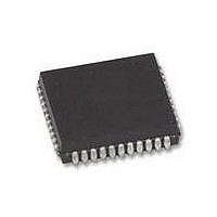
XR88C681J-F Exar Corporation, XR88C681J-F Datasheet - Page 70

XR88C681J-F
Manufacturer Part Number
XR88C681J-F
Description
IC UART CMOS DUAL 44PLCC
Manufacturer
Exar Corporation
Type
CMOS Dual Channel UARTr
Datasheet
1.XR88C681CP40-F.pdf
(101 pages)
Specifications of XR88C681J-F
Number Of Channels
2, DUART
Package / Case
44-LCC (J-Lead)
Features
*
Fifo's
1 Byte, 3 Byte
Voltage - Supply
5V
With Parallel Port
Yes
With Cmos
Yes
Mounting Type
Surface Mount
Data Rate
1 Mbps
Supply Voltage (max)
5.25 V
Supply Voltage (min)
4.75 V
Supply Current
15 mA
Maximum Operating Temperature
+ 85 C
Minimum Operating Temperature
- 40 C
Mounting Style
SMD/SMT
Operating Supply Voltage
5 V
Propagation Delay Time Ns
400 ns
No. Of Channels
2
Supply Voltage Range
4.75V To 5.25V
Operating Temperature Range
-40°C To +85°C
Digital Ic Case Style
PLCC
No. Of Pins
44
Filter Terminals
SMD
Rohs Compliant
Yes
Lead Free Status / RoHS Status
Lead free / RoHS Compliant
Lead Free Status / RoHS Status
Lead free / RoHS Compliant, Lead free / RoHS Compliant
Other names
1016-1329
Available stocks
Company
Part Number
Manufacturer
Quantity
Price
Company:
Part Number:
XR88C681J-F
Manufacturer:
Exar Corporation
Quantity:
10 000
The receiver functions by sensing the voltage level at the
RXDn input. When the far-end transmitter is idle, its TXDn
output
continuously “marking”. During this period the Receiver is
inactive and is not receiving or processing any data.
However, when the far-end transmitter sends the START
bit, (with its TXDn output toggling “low”), a receiver clock,
which is 16 times the baud rate (with the 16x clock), will
start sampling this START bit. If the receiver determines
that its RXDn input is still “low” after its 7th sample, then
the receiver hardware considers this signal to be a valid
START bit. If the RXDn input is not “low” at the 7th
sample, the Receiver will ignore this downward pulse as
“noise”. From this 7th sample on, the Receiver will
sample each successive bit at one bit-period intervals
(1/baud rate) with the 1x clock. The purpose of this 16x
Clock is then two-fold.
1. To verify that the detected “low” level in the RXDn input
is indeed a START bit.
Rev. 2.11
(and
Incoming
Serial Data
consequently,
RXDn
Figure 37. A Simplified Drawing of the Receiver Shift Register
Receive Shift Register
the
RXDn
and Receiver Holding Register
input)
Receiver Clock (from Timing Block)
is
70
Receive Holding
2. To establish the phase relationship between the 1x bit
Please note that if a 16X clock is selected for the receiver,
this over-sampling procedure occurs with each and every
start bit.
The receiver will continue to sample (and receive) each
bit of the character that follows the START bit, at one-bit
time intervals. Upon reception of the character’s MSB the
receiver will check parity (if programmed) or will sample
for the STOP bit.
condition at this time and the parity check (if any) was
valid; a successful reception of the character is
presumed; and the Receiver will prepare to sense and
oversample the occurrence of the START bit for the next
character.
Register
sampling clock, and the incoming serial data stream.
The idea is to sample each data bit in the middle of its
bit period.
RXCn
If the Receiver samples a mark
To Data Bus
To be read by the CPU


