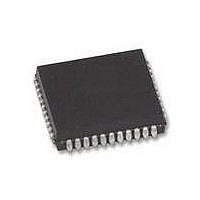
XR88C681J-F Exar Corporation, XR88C681J-F Datasheet - Page 68

XR88C681J-F
Manufacturer Part Number
XR88C681J-F
Description
IC UART CMOS DUAL 44PLCC
Manufacturer
Exar Corporation
Type
CMOS Dual Channel UARTr
Datasheet
1.XR88C681CP40-F.pdf
(101 pages)
Specifications of XR88C681J-F
Number Of Channels
2, DUART
Package / Case
44-LCC (J-Lead)
Features
*
Fifo's
1 Byte, 3 Byte
Voltage - Supply
5V
With Parallel Port
Yes
With Cmos
Yes
Mounting Type
Surface Mount
Data Rate
1 Mbps
Supply Voltage (max)
5.25 V
Supply Voltage (min)
4.75 V
Supply Current
15 mA
Maximum Operating Temperature
+ 85 C
Minimum Operating Temperature
- 40 C
Mounting Style
SMD/SMT
Operating Supply Voltage
5 V
Propagation Delay Time Ns
400 ns
No. Of Channels
2
Supply Voltage Range
4.75V To 5.25V
Operating Temperature Range
-40°C To +85°C
Digital Ic Case Style
PLCC
No. Of Pins
44
Filter Terminals
SMD
Rohs Compliant
Yes
Lead Free Status / RoHS Status
Lead free / RoHS Compliant
Lead Free Status / RoHS Status
Lead free / RoHS Compliant, Lead free / RoHS Compliant
Other names
1016-1329
Available stocks
Company
Part Number
Manufacturer
Quantity
Price
Company:
Part Number:
XR88C681J-F
Manufacturer:
Exar Corporation
Quantity:
10 000
F.3 28 Pin DIP Packaged DUARTs
The 28 pin DIP packaged devices have only two output
ports, OP0 and OP1. Hence the effect of the “SET
OUTPUT PORT BITS” and “CLEAR OUTPUT PORT
BITS” commands only effects these two pins. Additionally
-RTSA and -RTSB are the only alternative output port pin
functions available to this version of the XR88C681.
G. SERIAL CHANNELS A and B
Each serial channel of the DUART comprises a
full-duplex asynchronous receiver and transmitter. The
two channels can independently select their operating
frequency (from the BRG, the C/T, or an external clock) as
well as operating mode. Besides the normal mode in
which the receiver and transmitter of each channel
operate independently, the DUART can be configured to
operate in various looping modes, which are useful for
local and remote diagnostics, as well as in a wake up
mode used for multi-drop applications.
In this section certain symbols will be used to denote
certain aspects of the Transmitter and Receiver. The
definition of some of these symbols follows.
TXDn - Transmitter (Serial) Data Output for Channel n
TXCn - Transmitter Clock Signal for Channel n
RXDn - Receiver (Serial) Data Input for Channel n
RXCn - Receiver Clock Signal for Channel n
Figure 35. A Simplified Drawing Depicting the Transmit Shift Register and the Transmit Holding Register.
Rev. 2.11
From Data Bus.
Parallel Data from
the CPU
Transmitter Clock (from Timing Block)
Transmit Holding
TXCn
Register
68
This section of the data sheet discusses the resources
that are available to each channel. These resources are
listed here:
D Transmitter (Transmit Holding Register and Transmit
D Receiver (Receive Holding Register and Receive
D Status Register
D Mode Registers
D Command Register (See Section B.2, Command
D Clock Select Register (See Section D, Timing
G.1 Transmitter (TSR and THR)
The transmitter accepts parallel data from the CPU and
converts it to a serial bit stream where it is output at the
TXDn pin, adding start, stop and optional parity bits as
required by the asynchronous protocol.
Each transmitter consists of a Transmit Shift register (TSR)
and a Transmit Holding Register (THR).
actually a 1 byte FIFO. Figure 35 presents a simplified
illustration of the TSR and THR. The CPU initiates the
transmission of serial data by writing character data to the
THR. The character will be loaded into and processed
through the FIFO, until it reaches the TSR. During the
transition from the THR to the TSR, the character data is
serialized and is transmitted out of the chip via the TXDn pin.
Shift Register)
Shift Register)
Decoding)
Control Block)
Transmit Shift Register
Outgoing
Serial Data
TXDn
The THR is


