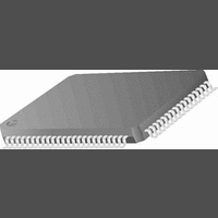
CR16MCS9VJE8 National Semiconductor, CR16MCS9VJE8 Datasheet - Page 110

CR16MCS9VJE8
Manufacturer Part Number
CR16MCS9VJE8
Description
16-Bit Microcontroller IC
Manufacturer
National Semiconductor
Datasheet
1.CR16MCS9VJE8.pdf
(156 pages)
Specifications of CR16MCS9VJE8
Controller Family/series
CR16X
Core Size
16 Bit
Program Memory Size
64K X 8 Flash
Digital Ic Case Style
PQFP
No. Of Pins
80
Mounting Type
Surface Mount
Clock Frequency
25MHz
Lead Free Status / RoHS Status
Contains lead / RoHS non-compliant
Available stocks
Company
Part Number
Manufacturer
Quantity
Price
Company:
Part Number:
CR16MCS9VJE8
Manufacturer:
ON
Quantity:
8 917
Company:
Part Number:
CR16MCS9VJE8-CBB
Manufacturer:
ON
Quantity:
846
Company:
Part Number:
CR16MCS9VJE8-CBC
Manufacturer:
ON
Quantity:
109
Company:
Part Number:
CR16MCS9VJE8-CBD
Manufacturer:
ON
Quantity:
17
Company:
Part Number:
CR16MCS9VJE8-CBE
Manufacturer:
ON
Quantity:
1 950
www.national.com
CRX
BUFFLOC
TSTPEN
“1” dominate state is “1”; recessive state is “0”
Control Receive. This bit configures the logic
level of the CAN receive pin CANRX.
“0” dominate state is “0”; recessive state is “1”
“1” dominate state is “1”; recessive state is “0”
Buffer Lock. With this bit the user can configure
the buffer lock function. If this feature is en-
abled, a buffer will be locked upon a successful
frame reception. The buffer will be unlocked
again by writing RX_READY in the buffer sta-
tus register, i.e., after reading data.
“0” lock function is disabled for all buffers
“1” lock function is enabled for all buffers
Time Sync Enable. The Time Sync bit enables
or disables the time stamp synchronization
function of the CR16CAN.
“0” Time synchronization disabled. The Time
Stamp counter value is not reset upon re-
Sequence of Data Bytes on the Bus
ID
Storage of Data Bytes
in the Buffer Memory
Data1
Data2
Figure 69. Data Direction Bit set to ‘0’
Data3
Data4
ADDR offset
110
0A
08
06
04
Data5
16
16
16
16
DDIR
Data6
Data1
Data3
Data5
Data7
Data Bytes
“1” Time synchronization enabled. The Time
Data Direction. By setting or resetting the DDIR
bit, the user can select the direction the data
bytes are transmitted and received. The
CR16CAN transmits and receives the CAN
data byte Data1 first and the data byte Data8
last (Data1, Data2,...,Data7, Data8).
If DDIR is set to “0” the data contents of a re-
ceived message is stored with the first byte at
the highest data address and the last data at
the lowest data address (see Figure69). The
same applies for transmitted data.
Data7
ception or transmission of a message to/
from buffer 0.
Stamp counter value is reset upon recep-
tion or transmission of a message to/from
buffer 0.
Data2
Data4
Data6
Data8
Data8
CRC
t


