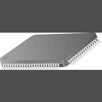
CR16MCS9VJE8 National Semiconductor, CR16MCS9VJE8 Datasheet - Page 139

CR16MCS9VJE8
Manufacturer Part Number
CR16MCS9VJE8
Description
16-Bit Microcontroller IC
Manufacturer
National Semiconductor
Datasheet
1.CR16MCS9VJE8.pdf
(156 pages)
Specifications of CR16MCS9VJE8
Controller Family/series
CR16X
Core Size
16 Bit
Program Memory Size
64K X 8 Flash
Digital Ic Case Style
PQFP
No. Of Pins
80
Mounting Type
Surface Mount
Clock Frequency
25MHz
Lead Free Status / RoHS Status
Contains lead / RoHS non-compliant
Available stocks
Company
Part Number
Manufacturer
Quantity
Price
Company:
Part Number:
CR16MCS9VJE8
Manufacturer:
ON
Quantity:
8 917
Company:
Part Number:
CR16MCS9VJE8-CBB
Manufacturer:
ON
Quantity:
846
Company:
Part Number:
CR16MCS9VJE8-CBC
Manufacturer:
ON
Quantity:
109
Company:
Part Number:
CR16MCS9VJE8-CBD
Manufacturer:
ON
Quantity:
17
Company:
Part Number:
CR16MCS9VJE8-CBE
Manufacturer:
ON
Quantity:
1 950
Analog Comparator Characteristics
Flash EEPROM Program Memory Programming
V
V
I
t
t
t
t
t
t
t
t
Symbol
CS
PWP
EWP
SDP
TTP
PAH
PEP
EDP
CHVP
Symbol
O S
CM
a. The programming pulse width is determined by the following equation:
b. The erase pulse width is determined by the following equation:
c. The program/erase start delay time is determined by the following equation:
d. The program/erase transition time is determined by the following equation:
e. The program/erase end delay time is determined by the following equation:
f. Cumulative program high voltage period for each row after erase t
t
FLPSLR register and FTPROG is the contents of the FLPROG register.
t
FLPSLR register and FTER is the contents of the FLERASE register.
t
FLPSLR register and FTSTART is the contents of the FLSTART register.
t
FLPSLR register and FTTRAN is the contents of the FLTRAN register.
t
register and FTEND is the contents of the FLEND register.
exposed to the programming voltage after the last erase cycle. It is the sum of all t
P W P
E W P
SDP
TTP
EDP
Programming pulse width
Erase pulse width
Charge pump power-up delay
Program/erase transition time
Programming address hold, new address setup
time
Charge pump enable hold time
Charge pump power hold time
Cumulative program high voltage period for each
row after erase.
Data retention
= T
= T
= T
= T
= T
Input Offset Voltage
Input Common Mode Voltage Range
DC Supply Current per Comparator (When
Enabled)
Response Time
clk
clk
clk
clk
clk
x (FTDIV+1) x (FTTRAN+1), where T
x (FTDIV+1) x (FTEND+1), where T
x (FTDIV+1) x (FTSTART+1), where T
x (FTDIV+1) x (FTPROG+1), where T
x (FTDIV+1) x 4 x (FTER+1), where T
f
Parameter
b
Parameter
a
d
c
e
clk
clk
is the system clock period, FTDIV is the contents of the FLPSLR
clk
clk
clk
is the system clock period, FTDIV is the contents of the
Vcc = 5V,
0.4V
V
1V Step / 100mV Overdrive
is the system clock period, FTDIV is the contents of the
is the system clock period, FTDIV is the contents of the
is the system clock period, FTDIV is the contents of the
CC
139
=5.5V
V
IN
Conditions
Conditions
V
CHVP
CC
– 1.5V
is the accumulated duration a flash cell is
HV
Min
0.4
after the last erase.
100
Min
30
10
1
5
2
1
5
-
-
Typ
V
100K
www.national.com
CC
Max
Max
250
40
25
-
-
-
-
-
-
25
1
-1.5
ms
clock
cycles
clock
cycles
ms
years
cycles
Units
s
s
s
s
Units
mV
V
A
s


