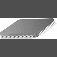
CR16MCS9VJE8 National Semiconductor, CR16MCS9VJE8 Datasheet - Page 121

CR16MCS9VJE8
Manufacturer Part Number
CR16MCS9VJE8
Description
16-Bit Microcontroller IC
Manufacturer
National Semiconductor
Datasheet
1.CR16MCS9VJE8.pdf
(156 pages)
Specifications of CR16MCS9VJE8
Controller Family/series
CR16X
Core Size
16 Bit
Program Memory Size
64K X 8 Flash
Digital Ic Case Style
PQFP
No. Of Pins
80
Mounting Type
Surface Mount
Clock Frequency
25MHz
Lead Free Status / RoHS Status
Contains lead / RoHS non-compliant
Available stocks
Company
Part Number
Manufacturer
Quantity
Price
Company:
Part Number:
CR16MCS9VJE8
Manufacturer:
ON
Quantity:
8 917
Company:
Part Number:
CR16MCS9VJE8-CBB
Manufacturer:
ON
Quantity:
846
Company:
Part Number:
CR16MCS9VJE8-CBC
Manufacturer:
ON
Quantity:
109
Company:
Part Number:
CR16MCS9VJE8-CBD
Manufacturer:
ON
Quantity:
17
Company:
Part Number:
CR16MCS9VJE8-CBE
Manufacturer:
ON
Quantity:
1 950
22.2.2
The ADCCNT1 register is a byte-wide, read/write register
used to enable the A/D Converter and its interrupts, and also
to control the reference voltage source. When writing to this
register, all reserved bits must be written with 0 for the A/D
Converter to function properly. Changing any bits other than
ADCEN (bit 0) is not allowed while the A/D Converter is ac-
tive (ADCST.BUSY or ADCCNT2.START set). Upon reset,
all non-reserved bits are cleared to 0. The register format is
shown below.
ADCEN
INTE
All reserved bits must be written with 0 for ADC to operate
properly.
22.2.3
The ADCCNT2 register is a byte-wide, read/write register
used to specify the A/D Converter operating mode and to
start conversion operations. All register fields other than the
START bit should be changed only while the A/D Converter
is inactive (START=0). Data written to the SCAN and CONT
fields is ignored if the START bit is already set. Upon reset,
the non-reserved bits of this register are cleared to 0. The
register format is shown below.
CHANNEL
7
START
6
Reserved
7
ADC Control 1 Register (ADCCNT1)
ADC Control 2 Register (ADCCNT2)
5
This register is initialized to 11 when a new
conversion is started (when ADCCNT2.START
is changed from 0 to 1) and is automatically in-
cremented every time a result is written to buff-
ers ADDATA0-ADDATA3. The result is a four-
entry cyclic FIFO buffer, with BUFPTR pointing
to the last entry written by the A/D Converter.
A/D Converter Enable. Setting this bit enables
the A/D Converter and allows a conversion to
be
(ADCCNT2.START). Clearing the ADCEN bit
disables the A/D Converter, terminates any
conversion in progress, and clears the ADC
status flags (ADCST.EOC, ADCST.BUSY,
ADCST.OVF, and ADCCNT2.START).
Interrupt Enable. This bit enables (1) or dis-
ables (0) A/D Converter interrupts. If enabled,
and interrupt occurs at the end of a conversion
sequence or when the ADC data buffer is full,
depending on the operating mode.
Channel Select. This 4-bit field selects one of
the twelve analog input channels as follows:
0000 = ACH0
0001 = ACH1
0010 = ACH2
0011 = ACH3
0100 = ACH4
0101 = ACH5
0110 = ACH6
0111 = ACH7
1000 = ACH8
1001 = ACH9
4
6
SCAN
started
3
5
INTE
2
by
CONT
4
Reserved
setting
1
3
the
CHANNEL
2
ADCEN
start
1
0
0
bit
121
CONT
SCAN
START
22.2.4
The ADCCNT3 register is a byte-wide, read/write register
used to specify the analog sampling time delay and the di-
vide-by factor for generating the ADC clock. This register
should be written only when the A/D Converter is disabled
(ADCCNT1.ADCEN=0). Upon reset, the non-reserved bits of
the ADCCNT3 register are cleared to 0. The register format
is shown below.
CDIV
DELAY
Reserved
7
ADC Control 3 Register (ADCCNT3)
PWREN
1010 = ACH10
1011 = ACH11
11XX = reserved
Continuous Conversion. When cleared to 0,
the A/D Converter stops operating upon com-
pletion of the programmed conversion cycle (a
single conversion or a sequence of four con-
versions on four channels). When set to 1, the
A/D Converter operates continuously by re-
peating the programmed conversion cycle.
Scan Mode. This 2-bit field selects the single-
conversion mode or 4-channel scan mode as
follows:
00 = single-conversion mode
01 = 4-channel scan mode
1X = reserved
Start Conversion. The software sets this bit to
1 to start a conversion or a 4-channel conver-
sion cycle. In the “continuous” mode, this bit re-
mains set until cleared by the software. In the
“single” (non-continuous) mode, the hardware
clears this bit upon completion of the pro-
grammed conversion cycle. The software
should not attempt to set this bit while the A/D
Converter is busy (ADCST.BUSY=1).
Clock Divide. This 3-bit field sets the divide-by
factor for generating the A/D Converter clock
from the system clock. The frequency of the A/
D Converter clock is equal to the system clock
divided by the programmed factor. The result-
ing A/D Converter clock frequency must be
less than or equal to 2 MHz. The divide-by fac-
tor is defined as follows:
000 = divide by 1
001 = divide by 2
010 = divide by 4
011 = divide by 8
100 = divide by 16
101 = divide by 32
Other = reserved
Sampling Time Delay. This 3-bit field defines
the number of A/D Converter clock cycles of
delay from the time that the input channel is se-
lected until the analog voltage is sampled. The
programmed delay should be sufficient, depen-
dent on the source impedance, to allow the
sampled signal to reach its final level before the
conversion begins. The delay is defined as fol-
lows:
6
5
DELAY
4
3
www.national.com
2
CDIV
1
0


