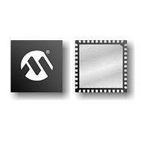
PIC16F724-E/MV Microchip Technology, PIC16F724-E/MV Datasheet - Page 106

PIC16F724-E/MV
Manufacturer Part Number
PIC16F724-E/MV
Description
7KB Flash Program, 1.8V-5.5V, 16MHz Internal Oscillator, 8b ADC, CCP, I2C/SPI, A
Manufacturer
Microchip Technology
Series
PIC® XLP™ 16Fr
Datasheet
1.AC164112.pdf
(302 pages)
Specifications of PIC16F724-E/MV
Processor Series
PIC16F
Core
PIC
Program Memory Type
Flash
Program Memory Size
7 KB
Data Ram Size
192 B
Interface Type
I2C, SPI, AUSART
Number Of Timers
3
Operating Supply Voltage
1.8 V to 5.5 V
Maximum Operating Temperature
+ 125 C
Mounting Style
SMD/SMT
Package / Case
UQFN-40
Development Tools By Supplier
MPLAB IDE Software
Minimum Operating Temperature
- 40 C
Core Processor
PIC
Core Size
8-Bit
Speed
20MHz
Connectivity
I²C, SPI, UART/USART
Peripherals
Brown-out Detect/Reset, POR, PWM, WDT
Number Of I /o
36
Eeprom Size
-
Ram Size
192 x 8
Voltage - Supply (vcc/vdd)
1.8 V ~ 5.5 V
Data Converters
A/D 14x8b
Oscillator Type
Internal
Operating Temperature
-40°C ~ 125°C
Lead Free Status / Rohs Status
Details
- Current page: 106 of 302
- Download datasheet (5Mb)
PIC16F72X/PIC16LF72X
9.3
For the ADC to meet its specified accuracy, the charge
holding capacitor (C
charge to the input channel voltage level. The Analog
Input model is shown in Figure 9-3. The source imped-
ance (R
impedance directly affect the time required to charge
the capacitor C
impedance varies over the device voltage (V
to Figure 9-3. The maximum recommended imped-
ance for analog sources is 10 kΩ. As the source
EQUATION 9-1:
DS41341E-page 106
The value for T
Solving for T
Therefore:
Note 1: The reference voltage (V
Assumptions:
V
V
V
Note: Where n = number of bits of the ADC.
S
2: The charge holding capacitor (C
3: The maximum recommended impedance for analog sources is 10 kΩ. This is required to meet the pin
A/D Acquisition Requirements
) and the internal sampling switch (R
AP P LI ED
AP P LI ED
AP P LI ED
T
leakage specification.
ACQ
T
C
ACQ
T
:
HOLD
C
C
⎛
⎝
⎛
⎜
⎝
⎛
⎜
⎝
=
Temperature
can be approximated with the following equations:
=
=
=
=
1
1 e
1 e
HOLD
=
=
=
. The sampling switch (R
2
ACQUISITION TIME EXAMPLE
4.42
–
–
–
1.12
–
–
ΜS
Amplifier Settling Time
T
2µs
C
10pF 1k
--------------------------
(
AMP
) must be allowed to fully
2
–
--------- -
–
-------- -
HOLD
RC
+
RC
ΜS
µs
T
Tc
n
+
C
1.12
+
⎞
⎟
⎠
⎞
⎟
⎠
(
+
1
T
1
(
C
) 1
=
R
=
T
ΜS
Ω
+
IC
C
–
=
V
V
+
+
[
+
REF
+
(
A PP LIE D
⎞
⎠
CHOLD
7k
50°C and external impedance of 10k
Temperature - 25°C
T
[
R
(
) has no effect on the equation, since it cancels itself out.
COFF
Ω
50°C- 25°C
=
SS
+
+
HOLD
DD
V
10k
CHOLD
R
), refer
⎛
⎝
S
1
+
) ln(1/511)
) is not discharged after each conversion.
Ω
SS
SS
–
Hold Capacitor Charging Time
)
)
)
) 0.05
--------------------------
(
ln(0.001957)
(
2
n
+
) 0.05µs/°C
1
ΜS
1
(
) 1
/°C
impedance is decreased, the acquisition time may be
decreased. After the analog input channel is selected
(or changed), an A/D acquisition must be done before
the conversion can be started. To calculate the mini-
mum acquisition time, Equation 9-1 may be used. This
equation assumes that 1/2 LSb error is used (256 steps
for the ADC). The 1/2 LSb error is the maximum error
allowed for the ADC to meet its specified resolution.
–
)
⎞
⎠
]
;[1] V
;[2] V
;combining [1] and [2]
)
]
Ω
CHOLD
CHOLD
5.0V V
+
charged to within 1/2 lsb
charge response to V
DD
Temperature Coefficient
© 2009 Microchip Technology Inc.
APPLIED
Related parts for PIC16F724-E/MV
Image
Part Number
Description
Manufacturer
Datasheet
Request
R

Part Number:
Description:
IC PIC MCU FLASH 4KX14 44-QFN
Manufacturer:
Microchip Technology
Datasheet:

Part Number:
Description:
IC PIC MCU FLASH 4KX14 44TQFP
Manufacturer:
Microchip Technology
Datasheet:

Part Number:
Description:
IC PIC MCU FLASH 4KX14 40-DIP
Manufacturer:
Microchip Technology
Datasheet:

Part Number:
Description:
7KB Flash Program, 1.8V-5.5V, 16MHz Internal Oscillator, 8b ADC, CCP, I2C/SPI, A
Manufacturer:
Microchip Technology
Datasheet:

Part Number:
Description:
7KB Flash Program, 1.8V-5.5V, 16MHz Internal Oscillator, 8b ADC, CCP, I2C/SPI, A
Manufacturer:
Microchip Technology
Datasheet:

Part Number:
Description:
7KB Flash Program, 1.8V-5.5V, 16MHz Internal Oscillator, 8b ADC, CCP, I2C/SPI, A
Manufacturer:
Microchip Technology
Datasheet:

Part Number:
Description:
7KB Flash Program, 1.8V-5.5V, 16MHz Internal Oscillator, 8b ADC, CCP, I2C/SPI, A
Manufacturer:
Microchip Technology

Part Number:
Description:
IC PIC MCU FLASH 2KX14 28-QFN
Manufacturer:
Microchip Technology
Datasheet:

Part Number:
Description:
IC PIC MCU FLASH 2KX14 28-SOIC
Manufacturer:
Microchip Technology
Datasheet:

Part Number:
Description:
IC PIC MCU FLASH 2KX14 28DIP
Manufacturer:
Microchip Technology
Datasheet:

Part Number:
Description:
IC PIC MCU FLASH 2KX14 28-SOIC
Manufacturer:
Microchip Technology
Datasheet:

Part Number:
Description:
IC PIC MCU FLASH 2KX14 28QFN
Manufacturer:
Microchip Technology

Part Number:
Description:
IC PIC MCU FLASH 2KX14 28SSOP
Manufacturer:
Microchip Technology

Part Number:
Description:
IC PIC MCU FLASH 2KX14 8-SSOP
Manufacturer:
Microchip Technology
Datasheet:

Part Number:
Description:
IC PIC MCU FLASH 2KX14 28-SSOP
Manufacturer:
Microchip Technology
Datasheet:


