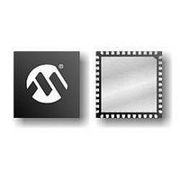
PIC16F724-E/MV Microchip Technology, PIC16F724-E/MV Datasheet - Page 73

PIC16F724-E/MV
Manufacturer Part Number
PIC16F724-E/MV
Description
7KB Flash Program, 1.8V-5.5V, 16MHz Internal Oscillator, 8b ADC, CCP, I2C/SPI, A
Manufacturer
Microchip Technology
Series
PIC® XLP™ 16Fr
Datasheet
1.AC164112.pdf
(302 pages)
Specifications of PIC16F724-E/MV
Processor Series
PIC16F
Core
PIC
Program Memory Type
Flash
Program Memory Size
7 KB
Data Ram Size
192 B
Interface Type
I2C, SPI, AUSART
Number Of Timers
3
Operating Supply Voltage
1.8 V to 5.5 V
Maximum Operating Temperature
+ 125 C
Mounting Style
SMD/SMT
Package / Case
UQFN-40
Development Tools By Supplier
MPLAB IDE Software
Minimum Operating Temperature
- 40 C
Core Processor
PIC
Core Size
8-Bit
Speed
20MHz
Connectivity
I²C, SPI, UART/USART
Peripherals
Brown-out Detect/Reset, POR, PWM, WDT
Number Of I /o
36
Eeprom Size
-
Ram Size
192 x 8
Voltage - Supply (vcc/vdd)
1.8 V ~ 5.5 V
Data Converters
A/D 14x8b
Oscillator Type
Internal
Operating Temperature
-40°C ~ 125°C
Lead Free Status / Rohs Status
Details
- Current page: 73 of 302
- Download datasheet (5Mb)
6.4
PORTC is a 8-bit wide, bidirectional port. The
corresponding
(Register 6-11). Setting a TRISC bit (= 1) will make the
corresponding PORTC pin an input (i.e., put the
corresponding output driver in a High-Impedance mode).
Clearing a TRISC bit (= 0) will make the corresponding
PORTC pin an output (i.e., enable the output driver and
put the contents of the output latch on the selected pin).
Example 6-3 shows how to initialize PORTC.
Reading the PORTC register (Register 6-10) reads the
status of the pins, whereas writing to it will write to the
PORT latch. All write operations are read-modify-write
operations. Therefore, a write to a port implies that the
port pins are read, this value is modified and then written
to the PORT data latch.
REGISTER 6-10:
REGISTER 6-11:
© 2009 Microchip Technology Inc.
bit 7
Legend:
R = Readable bit
-n = Value at POR
bit 7-0
bit 7
Legend:
R = Readable bit
-n = Value at POR
bit 7-0
TRISC7
R/W-1
R/W-x
RC7
PORTC and TRISC Registers
data
RC<7:0>: PORTC General Purpose I/O Pin bits
1 = Port pin is > V
0 = Port pin is < V
TRISC<7:0>: PORTC Tri-State Control bits
1 = PORTC pin configured as an input (tri-stated)
0 = PORTC pin configured as an output
TRISC6
R/W-1
R/W-x
RC6
PORTC: PORTC REGISTER
TRISC: PORTC TRI-STATE REGISTER
direction
W = Writable bit
‘1’ = Bit is set
W = Writable bit
‘1’ = Bit is set
TRISC5
register
IH
IL
R/W-1
R/W-x
RC5
is
TRISC
TRISC4
R/W-1
R/W-x
RC4
PIC16F72X/PIC16LF72X
U = Unimplemented bit, read as ‘0’
U = Unimplemented bit, read as ‘0’
‘0’ = Bit is cleared
‘0’ = Bit is cleared
TRISC3
R/W-1
R/W-x
The TRISC register (Register 6-11) controls the PORTC
pin output drivers, even when they are being used as
analog inputs. The user should ensure the bits in the
TRISC register are maintained set when using them as
analog inputs. I/O pins configured as analog input always
read ‘0’.
EXAMPLE 6-3:
The location of the CCP2 function is controlled by the
CCP2SEL bit in the APFCON register (refer to
Register 6-1)
RC3
BANKSEL PORTC
CLRF
BANKSEL TRISC
MOVLW
MOVWF
PORTC
B‘00001100’
TRISC
TRISC2
R/W-x
R/W-1
RC2
INITIALIZING PORTC
;
;Init PORTC
;
;Set RC<3:2> as inputs
;and set RC<7:4,1:0>
;as outputs
x = Bit is unknown
x = Bit is unknown
TRISC1
R/W-x
R/W-1
RC1
DS41341E-page 73
TRISC0
R/W-1
R/W-x
RC0
bit 0
bit 0
Related parts for PIC16F724-E/MV
Image
Part Number
Description
Manufacturer
Datasheet
Request
R

Part Number:
Description:
IC PIC MCU FLASH 4KX14 44-QFN
Manufacturer:
Microchip Technology
Datasheet:

Part Number:
Description:
IC PIC MCU FLASH 4KX14 44TQFP
Manufacturer:
Microchip Technology
Datasheet:

Part Number:
Description:
IC PIC MCU FLASH 4KX14 40-DIP
Manufacturer:
Microchip Technology
Datasheet:

Part Number:
Description:
7KB Flash Program, 1.8V-5.5V, 16MHz Internal Oscillator, 8b ADC, CCP, I2C/SPI, A
Manufacturer:
Microchip Technology
Datasheet:

Part Number:
Description:
7KB Flash Program, 1.8V-5.5V, 16MHz Internal Oscillator, 8b ADC, CCP, I2C/SPI, A
Manufacturer:
Microchip Technology
Datasheet:

Part Number:
Description:
7KB Flash Program, 1.8V-5.5V, 16MHz Internal Oscillator, 8b ADC, CCP, I2C/SPI, A
Manufacturer:
Microchip Technology
Datasheet:

Part Number:
Description:
7KB Flash Program, 1.8V-5.5V, 16MHz Internal Oscillator, 8b ADC, CCP, I2C/SPI, A
Manufacturer:
Microchip Technology

Part Number:
Description:
IC PIC MCU FLASH 2KX14 28-QFN
Manufacturer:
Microchip Technology
Datasheet:

Part Number:
Description:
IC PIC MCU FLASH 2KX14 28-SOIC
Manufacturer:
Microchip Technology
Datasheet:

Part Number:
Description:
IC PIC MCU FLASH 2KX14 28DIP
Manufacturer:
Microchip Technology
Datasheet:

Part Number:
Description:
IC PIC MCU FLASH 2KX14 28-SOIC
Manufacturer:
Microchip Technology
Datasheet:

Part Number:
Description:
IC PIC MCU FLASH 2KX14 28QFN
Manufacturer:
Microchip Technology

Part Number:
Description:
IC PIC MCU FLASH 2KX14 28SSOP
Manufacturer:
Microchip Technology

Part Number:
Description:
IC PIC MCU FLASH 2KX14 8-SSOP
Manufacturer:
Microchip Technology
Datasheet:

Part Number:
Description:
IC PIC MCU FLASH 2KX14 28-SSOP
Manufacturer:
Microchip Technology
Datasheet:


