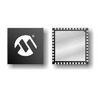
PIC16F724-E/MV Microchip Technology, PIC16F724-E/MV Datasheet - Page 55

PIC16F724-E/MV
Manufacturer Part Number
PIC16F724-E/MV
Description
7KB Flash Program, 1.8V-5.5V, 16MHz Internal Oscillator, 8b ADC, CCP, I2C/SPI, A
Manufacturer
Microchip Technology
Series
PIC® XLP™ 16Fr
Datasheet
1.AC164112.pdf
(302 pages)
Specifications of PIC16F724-E/MV
Processor Series
PIC16F
Core
PIC
Program Memory Type
Flash
Program Memory Size
7 KB
Data Ram Size
192 B
Interface Type
I2C, SPI, AUSART
Number Of Timers
3
Operating Supply Voltage
1.8 V to 5.5 V
Maximum Operating Temperature
+ 125 C
Mounting Style
SMD/SMT
Package / Case
UQFN-40
Development Tools By Supplier
MPLAB IDE Software
Minimum Operating Temperature
- 40 C
Core Processor
PIC
Core Size
8-Bit
Speed
20MHz
Connectivity
I²C, SPI, UART/USART
Peripherals
Brown-out Detect/Reset, POR, PWM, WDT
Number Of I /o
36
Eeprom Size
-
Ram Size
192 x 8
Voltage - Supply (vcc/vdd)
1.8 V ~ 5.5 V
Data Converters
A/D 14x8b
Oscillator Type
Internal
Operating Temperature
-40°C ~ 125°C
Lead Free Status / Rohs Status
Details
- Current page: 55 of 302
- Download datasheet (5Mb)
6.2.1
The ANSELA register (Register 6-4) is used to
configure the Input mode of an I/O pin to analog.
Setting the appropriate ANSELA bit high will cause all
digital reads on the pin to be read as ‘0’ and allow
analog functions on the pin to operate correctly.
The state of the ANSELA bits has no affect on digital
output functions. A pin with TRIS clear and ANSEL set
will still operate as a digital output, but the Input mode
will be analog. This can cause unexpected behavior
when executing read-modify-write instructions on the
affected port.
REGISTER 6-4:
© 2009 Microchip Technology Inc.
bit 7
Legend:
R = Readable bit
-n = Value at POR
bit 7-6
bit 5-0
Note 1:
U-0
—
ANSELA REGISTER
When setting a pin to an analog input, the corresponding TRIS bit must be set to Input mode in order to
allow external control of the voltage on the pin.
Unimplemented: Read as ‘0’
ANSA<5:0>: Analog Select between Analog or Digital Function on pins RA<5:0>, respectively
0 = Digital I/O. Pin is assigned to port or Digital special function.
1 = Analog input. Pin is assigned as analog input
U-0
—
ANSELA: PORTA ANALOG SELECT REGISTER
W = Writable bit
‘1’ = Bit is set
ANSA5
R/W-1
ANSA4
R/W-1
PIC16F72X/PIC16LF72X
U = Unimplemented bit, read as ‘0’
‘0’ = Bit is cleared
ANSA3
R/W-1
(1)
. Digital Input buffer disabled.
ANSA2
R/W-1
x = Bit is unknown
ANSA1
R/W-1
DS41341E-page 55
ANSA0
R/W-1
bit 0
Related parts for PIC16F724-E/MV
Image
Part Number
Description
Manufacturer
Datasheet
Request
R

Part Number:
Description:
IC PIC MCU FLASH 4KX14 44-QFN
Manufacturer:
Microchip Technology
Datasheet:

Part Number:
Description:
IC PIC MCU FLASH 4KX14 44TQFP
Manufacturer:
Microchip Technology
Datasheet:

Part Number:
Description:
IC PIC MCU FLASH 4KX14 40-DIP
Manufacturer:
Microchip Technology
Datasheet:

Part Number:
Description:
7KB Flash Program, 1.8V-5.5V, 16MHz Internal Oscillator, 8b ADC, CCP, I2C/SPI, A
Manufacturer:
Microchip Technology
Datasheet:

Part Number:
Description:
7KB Flash Program, 1.8V-5.5V, 16MHz Internal Oscillator, 8b ADC, CCP, I2C/SPI, A
Manufacturer:
Microchip Technology
Datasheet:

Part Number:
Description:
7KB Flash Program, 1.8V-5.5V, 16MHz Internal Oscillator, 8b ADC, CCP, I2C/SPI, A
Manufacturer:
Microchip Technology
Datasheet:

Part Number:
Description:
7KB Flash Program, 1.8V-5.5V, 16MHz Internal Oscillator, 8b ADC, CCP, I2C/SPI, A
Manufacturer:
Microchip Technology

Part Number:
Description:
IC PIC MCU FLASH 2KX14 28-QFN
Manufacturer:
Microchip Technology
Datasheet:

Part Number:
Description:
IC PIC MCU FLASH 2KX14 28-SOIC
Manufacturer:
Microchip Technology
Datasheet:

Part Number:
Description:
IC PIC MCU FLASH 2KX14 28DIP
Manufacturer:
Microchip Technology
Datasheet:

Part Number:
Description:
IC PIC MCU FLASH 2KX14 28-SOIC
Manufacturer:
Microchip Technology
Datasheet:

Part Number:
Description:
IC PIC MCU FLASH 2KX14 28QFN
Manufacturer:
Microchip Technology

Part Number:
Description:
IC PIC MCU FLASH 2KX14 28SSOP
Manufacturer:
Microchip Technology

Part Number:
Description:
IC PIC MCU FLASH 2KX14 8-SSOP
Manufacturer:
Microchip Technology
Datasheet:

Part Number:
Description:
IC PIC MCU FLASH 2KX14 28-SSOP
Manufacturer:
Microchip Technology
Datasheet:


