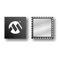
PIC16F724-E/MV Microchip Technology, PIC16F724-E/MV Datasheet - Page 177

PIC16F724-E/MV
Manufacturer Part Number
PIC16F724-E/MV
Description
7KB Flash Program, 1.8V-5.5V, 16MHz Internal Oscillator, 8b ADC, CCP, I2C/SPI, A
Manufacturer
Microchip Technology
Series
PIC® XLP™ 16Fr
Datasheet
1.AC164112.pdf
(302 pages)
Specifications of PIC16F724-E/MV
Processor Series
PIC16F
Core
PIC
Program Memory Type
Flash
Program Memory Size
7 KB
Data Ram Size
192 B
Interface Type
I2C, SPI, AUSART
Number Of Timers
3
Operating Supply Voltage
1.8 V to 5.5 V
Maximum Operating Temperature
+ 125 C
Mounting Style
SMD/SMT
Package / Case
UQFN-40
Development Tools By Supplier
MPLAB IDE Software
Minimum Operating Temperature
- 40 C
Core Processor
PIC
Core Size
8-Bit
Speed
20MHz
Connectivity
I²C, SPI, UART/USART
Peripherals
Brown-out Detect/Reset, POR, PWM, WDT
Number Of I /o
36
Eeprom Size
-
Ram Size
192 x 8
Voltage - Supply (vcc/vdd)
1.8 V ~ 5.5 V
Data Converters
A/D 14x8b
Oscillator Type
Internal
Operating Temperature
-40°C ~ 125°C
Lead Free Status / Rohs Status
Details
- Current page: 177 of 302
- Download datasheet (5Mb)
17.2
The SSP module, in I
functions, except general call support. It provides
interrupts on Start and Stop bits in hardware to facilitate
firmware implementations of the master functions. The
SSP module implements the I
specifications:
• I
• I
• Start and Stop bit interrupts enabled to support
• Address masking
Two pins are used for data transfer; the SCL pin (clock
line) and the SDA pin (data line). The user must
configure the two pin’s data direction bits as inputs in
the appropriate TRIS register. Upon enabling I
mode, the I
controlled by the SMP bit of SSPSTAT register. The
SSP module functions are enabled by setting the
SSPEN bit of SSPCON register.
Data is sampled on the rising edge and shifted out on
the falling edge of the clock. This ensures that the SDA
signal is valid during the SCL high time. The SCL clock
input must have minimum high and low times for proper
operation.
Specifications”.
FIGURE 17-7:
© 2009 Microchip Technology Inc.
firmware Master mode
2
2
C Slave mode (7-bit address)
C Slave mode (10-bit address)
SDA
SCL
I
2
C Mode
2
C slew rate limiters in the I/O pads are
Refer
Read
Shift
Clock
MSb
to
2
I
DIAGRAM
2
C mode, implements all slave
SSPMSK Reg
SSPADD Reg
Match Detect
C™ MODE BLOCK
Stop bit Detect
SSPBUF Reg
SSPSR Reg
Section 23.0
Start and
2
C Standard mode
LSb
Write
Addr Match
Internal
Data Bus
“Electrical
2
C
PIC16F72X/PIC16LF72X
FIGURE 17-8:
The SSP module has six registers for I
They are:
• SSP Control (SSPCON) register
• SSP Status (SSPSTAT) register
• Serial Receive/Transmit Buffer (SSPBUF) register
• SSP Shift Register (SSPSR), not directly
• SSP Address (SSPADD) register
• SSP Address Mask (SSPMSK) register
17.2.1
Selection of I
SSPCON register set, forces the SCL and SDA pins to
be open drain, provided these pins are programmed as
inputs by setting the appropriate TRISC bits. The SSP
module will override the input state with the output
data, when required, such as for Acknowledge and
slave-transmitter sequences.
accessible
Note:
Master
HARDWARE SETUP
Pull-up
externally to the SCL and SDA pins for
proper operation of the I
SDA
SCL
2
C mode, with the SSPEN bit of the
V
resistors
TYPICAL I
CONNECTIONS
DD
V
DD
must
2
DS41341E-page 177
C™
2
C module.
SDA
SDA
SCL
SCL
(optional)
Slave 1
Slave 2
be
2
C operation.
provided
Related parts for PIC16F724-E/MV
Image
Part Number
Description
Manufacturer
Datasheet
Request
R

Part Number:
Description:
IC PIC MCU FLASH 4KX14 44-QFN
Manufacturer:
Microchip Technology
Datasheet:

Part Number:
Description:
IC PIC MCU FLASH 4KX14 44TQFP
Manufacturer:
Microchip Technology
Datasheet:

Part Number:
Description:
IC PIC MCU FLASH 4KX14 40-DIP
Manufacturer:
Microchip Technology
Datasheet:

Part Number:
Description:
7KB Flash Program, 1.8V-5.5V, 16MHz Internal Oscillator, 8b ADC, CCP, I2C/SPI, A
Manufacturer:
Microchip Technology
Datasheet:

Part Number:
Description:
7KB Flash Program, 1.8V-5.5V, 16MHz Internal Oscillator, 8b ADC, CCP, I2C/SPI, A
Manufacturer:
Microchip Technology
Datasheet:

Part Number:
Description:
7KB Flash Program, 1.8V-5.5V, 16MHz Internal Oscillator, 8b ADC, CCP, I2C/SPI, A
Manufacturer:
Microchip Technology
Datasheet:

Part Number:
Description:
7KB Flash Program, 1.8V-5.5V, 16MHz Internal Oscillator, 8b ADC, CCP, I2C/SPI, A
Manufacturer:
Microchip Technology

Part Number:
Description:
IC PIC MCU FLASH 2KX14 28-QFN
Manufacturer:
Microchip Technology
Datasheet:

Part Number:
Description:
IC PIC MCU FLASH 2KX14 28-SOIC
Manufacturer:
Microchip Technology
Datasheet:

Part Number:
Description:
IC PIC MCU FLASH 2KX14 28DIP
Manufacturer:
Microchip Technology
Datasheet:

Part Number:
Description:
IC PIC MCU FLASH 2KX14 28-SOIC
Manufacturer:
Microchip Technology
Datasheet:

Part Number:
Description:
IC PIC MCU FLASH 2KX14 28QFN
Manufacturer:
Microchip Technology

Part Number:
Description:
IC PIC MCU FLASH 2KX14 28SSOP
Manufacturer:
Microchip Technology

Part Number:
Description:
IC PIC MCU FLASH 2KX14 8-SSOP
Manufacturer:
Microchip Technology
Datasheet:

Part Number:
Description:
IC PIC MCU FLASH 2KX14 28-SSOP
Manufacturer:
Microchip Technology
Datasheet:


