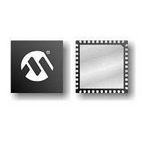
PIC16F724-E/MV Microchip Technology, PIC16F724-E/MV Datasheet - Page 27

PIC16F724-E/MV
Manufacturer Part Number
PIC16F724-E/MV
Description
7KB Flash Program, 1.8V-5.5V, 16MHz Internal Oscillator, 8b ADC, CCP, I2C/SPI, A
Manufacturer
Microchip Technology
Series
PIC® XLP™ 16Fr
Datasheet
1.AC164112.pdf
(302 pages)
Specifications of PIC16F724-E/MV
Processor Series
PIC16F
Core
PIC
Program Memory Type
Flash
Program Memory Size
7 KB
Data Ram Size
192 B
Interface Type
I2C, SPI, AUSART
Number Of Timers
3
Operating Supply Voltage
1.8 V to 5.5 V
Maximum Operating Temperature
+ 125 C
Mounting Style
SMD/SMT
Package / Case
UQFN-40
Development Tools By Supplier
MPLAB IDE Software
Minimum Operating Temperature
- 40 C
Core Processor
PIC
Core Size
8-Bit
Speed
20MHz
Connectivity
I²C, SPI, UART/USART
Peripherals
Brown-out Detect/Reset, POR, PWM, WDT
Number Of I /o
36
Eeprom Size
-
Ram Size
192 x 8
Voltage - Supply (vcc/vdd)
1.8 V ~ 5.5 V
Data Converters
A/D 14x8b
Oscillator Type
Internal
Operating Temperature
-40°C ~ 125°C
Lead Free Status / Rohs Status
Details
- Current page: 27 of 302
- Download datasheet (5Mb)
2.2.2.1
The STATUS register, shown in Register 2-1, contains:
• the arithmetic status of the ALU
• the Reset status
• the bank select bits for data memory (SRAM)
The STATUS register can be the destination for any
instruction, like any other register. If the STATUS
register is the destination for an instruction that affects
the Z, DC or C bits, then the write to these three bits is
disabled. These bits are set or cleared according to the
device logic. Furthermore, the TO and PD bits are not
writable. Therefore, the result of an instruction with the
STATUS register as destination may be different than
intended.
REGISTER 2-1:
© 2009 Microchip Technology Inc.
bit 7
Legend:
R = Readable bit
-n = Value at POR
bit 7
bit 6-5
bit 4
bit 3
bit 2
bit 1
bit 0
Note 1:
R/W-0
IRP
For Borrow, the polarity is reversed. A subtraction is executed by adding the two’s complement of the
second operand. For rotate (RRF, RLF) instructions, this bit is loaded with either the high-order or low-order
bit of the source register.
STATUS Register
IRP: Register Bank Select bit (used for indirect addressing)
1 = Bank 2, 3 (100h-1FFh)
0 = Bank 0, 1 (00h-FFh)
RP<1:0>: Register Bank Select bits (used for direct addressing)
00 = Bank 0 (00h-7Fh)
01 = Bank 1 (80h-FFh)
10 = Bank 2 (100h-17Fh)
11 = Bank 3 (180h-1FFh)
TO: Time-out bit
1 = After power-up, CLRWDT instruction or SLEEP instruction
0 = A WDT time-out occurred
PD: Power-down bit
1 = After power-up or by the CLRWDT instruction
0 = By execution of the SLEEP instruction
Z: Zero bit
1 = The result of an arithmetic or logic operation is zero
0 = The result of an arithmetic or logic operation is not zero
DC: Digit Carry/Digit Borrow bit (ADDWF, ADDLW,SUBLW,SUBWF instructions)
1 = A carry-out from the 4th low-order bit of the result occurred
0 = No carry-out from the 4th low-order bit of the result
C: Carry/Borrow bit
1 = A carry-out from the Most Significant bit of the result occurred
0 = No carry-out from the Most Significant bit of the result occurred
R/W-0
RP1
STATUS: STATUS REGISTER
W = Writable bit
‘1’ = Bit is set
R/W-0
RP0
(1)
(ADDWF, ADDLW, SUBLW, SUBWF instructions)
R-1
TO
PIC16F72X/PIC16LF72X
U = Unimplemented bit, read as ‘0’
‘0’ = Bit is cleared
For example, CLRF STATUS will clear the upper three
bits and set the Z bit. This leaves the STATUS register
as ‘000u u1uu’ (where u = unchanged).
It is recommended, therefore, that only BCF, BSF,
SWAPF and MOVWF instructions are used to alter the
STATUS register, because these instructions do not
affect any Status bits. For other instructions not
affecting any Status bits (Refer to Section 21.0
“Instruction Set Summary”).
R-1
PD
Note 1: The C and DC bits operate as Borrow and
Digit Borrow out bits, respectively, in
subtraction.
R/W-x
Z
(1)
x = Bit is unknown
R/W-x
(1)
DC
(1)
DS41341E-page 27
R/W-x
C
(1)
bit 0
Related parts for PIC16F724-E/MV
Image
Part Number
Description
Manufacturer
Datasheet
Request
R

Part Number:
Description:
IC PIC MCU FLASH 4KX14 44-QFN
Manufacturer:
Microchip Technology
Datasheet:

Part Number:
Description:
IC PIC MCU FLASH 4KX14 44TQFP
Manufacturer:
Microchip Technology
Datasheet:

Part Number:
Description:
IC PIC MCU FLASH 4KX14 40-DIP
Manufacturer:
Microchip Technology
Datasheet:

Part Number:
Description:
7KB Flash Program, 1.8V-5.5V, 16MHz Internal Oscillator, 8b ADC, CCP, I2C/SPI, A
Manufacturer:
Microchip Technology
Datasheet:

Part Number:
Description:
7KB Flash Program, 1.8V-5.5V, 16MHz Internal Oscillator, 8b ADC, CCP, I2C/SPI, A
Manufacturer:
Microchip Technology
Datasheet:

Part Number:
Description:
7KB Flash Program, 1.8V-5.5V, 16MHz Internal Oscillator, 8b ADC, CCP, I2C/SPI, A
Manufacturer:
Microchip Technology
Datasheet:

Part Number:
Description:
7KB Flash Program, 1.8V-5.5V, 16MHz Internal Oscillator, 8b ADC, CCP, I2C/SPI, A
Manufacturer:
Microchip Technology

Part Number:
Description:
IC PIC MCU FLASH 2KX14 28-QFN
Manufacturer:
Microchip Technology
Datasheet:

Part Number:
Description:
IC PIC MCU FLASH 2KX14 28-SOIC
Manufacturer:
Microchip Technology
Datasheet:

Part Number:
Description:
IC PIC MCU FLASH 2KX14 28DIP
Manufacturer:
Microchip Technology
Datasheet:

Part Number:
Description:
IC PIC MCU FLASH 2KX14 28-SOIC
Manufacturer:
Microchip Technology
Datasheet:

Part Number:
Description:
IC PIC MCU FLASH 2KX14 28QFN
Manufacturer:
Microchip Technology

Part Number:
Description:
IC PIC MCU FLASH 2KX14 28SSOP
Manufacturer:
Microchip Technology

Part Number:
Description:
IC PIC MCU FLASH 2KX14 8-SSOP
Manufacturer:
Microchip Technology
Datasheet:

Part Number:
Description:
IC PIC MCU FLASH 2KX14 28-SSOP
Manufacturer:
Microchip Technology
Datasheet:


