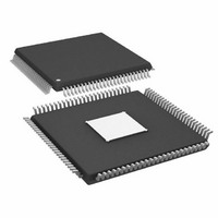
AD9957BSVZ Analog Devices Inc, AD9957BSVZ Datasheet - Page 17

AD9957BSVZ
Manufacturer Part Number
AD9957BSVZ
Description
IC DDS 1GSPS 14BIT IQ 100TQFP
Manufacturer
Analog Devices Inc
Datasheet
1.AD9957BSVZ-REEL.pdf
(64 pages)
Specifications of AD9957BSVZ
Resolution (bits)
14 b
Master Fclk
1GHz
Tuning Word Width (bits)
32 b
Voltage - Supply
1.8V, 3.3V
Operating Temperature
-40°C ~ 85°C
Mounting Type
Surface Mount
Package / Case
100-TQFP Exposed Pad, 100-eTQFP, 100-HTQFP, 100-VQFP
Frequency Range
60MHz To 1GHz
Rf Type
Quadrature
Supply Voltage Range
1.71V To 1.89V, 3.135V To 3.465
Rf Ic Case Style
TQFP
No. Of Pins
100
Operating Temperature Range
-40°C To +85°C
Operating Temperature (max)
85C
Operating Temperature (min)
-40C
Pin Count
100
Mounting
Surface Mount
Case Height
1mm
Screening Level
Industrial
Lead Free Status / RoHS Status
Lead free / RoHS Compliant
For Use With
AD9957/PCBZ - BOARD EVAL AD9957 QUADRATURE MOD
Lead Free Status / Rohs Status
Compliant
Available stocks
Company
Part Number
Manufacturer
Quantity
Price
Company:
Part Number:
AD9957BSVZ
Manufacturer:
AD
Quantity:
1 200
Company:
Part Number:
AD9957BSVZ
Manufacturer:
Analog Devices Inc
Quantity:
10 000
Part Number:
AD9957BSVZ
Manufacturer:
ADI/亚德诺
Quantity:
20 000
Company:
Part Number:
AD9957BSVZ-REEL
Manufacturer:
Analog Devices Inc
Quantity:
10 000
Part Number:
AD9957BSVZ-REEL
Manufacturer:
ADI/亚德诺
Quantity:
20 000
QUADRATURE MODULATION MODE
A block diagram of the AD9957 operating in QDUC mode is
shown in Figure 26; grayed items are inactive. The parallel input
accepts 18-bit I- and Q-words in time-interleaved fashion. That
is, an 18-bit I-word is followed by an 18-bit Q-word, then the
next 18-bit I-word, and so on. One 18-bit I-word and one 18-bit
Q-word together comprise one internal sample. The data assem-
bler and formatter de-interleave the I- and Q-words so that each
sample propagates along the internal data pathway in parallel
fashion. Both I and Q data paths are active; the parallel data
clock (PDCLK) serves to synchronize the input of I/Q data to
the AD9957.
TxENABLE
PDCLK
I/Q IN
FTW
18
PW
TIMING AND CONTROL
PROGRAMMING
PARALLEL DATA
REGISTERS
3
18
16
16
18
QS
Q
IS
I
SERIAL I/O
PORT
INTERNAL CLOCK TIMING AND CONTROL
Figure 26. Quadrature Modulation Mode
I Q
RAM
IS QS
Rev. B | Page 17 of 64
OSK
AD9957
cos (ωt+θ)
θ
ω
sin (ωt+θ)
CLOCK
CONTROL
DDS
POWER
DOWN
The PROFILE and I/O_UPDATE pins are also synchronous to
the PDCLK.
The DDS core provides a quadrature (sine and cosine) local
oscillator signal to the quadrature modulator, where the
interpolated I and Q samples are multiplied by the respective
phase of the carrier and summed together, producing a
quadrature modulated data stream. This data stream is routed
through the inverse sinc filter (optionally), and the output
scaling multiplier. Then it is applied to the 14-bit DAC to
produce the quadrature modulated analog output signal.
2
2
SYSCLK
DAC GAIN
PLL
÷2
8
OUTPUT
FACTOR
SCALE
8-BIT
AUX
DAC
14-BIT
DAC
DAC_RSET
IOUT
IOUT
REFCLK_OUT
REF_CLK
REF_CLK
XTAL_SEL
AD9957


