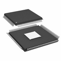
AD9957BSVZ Analog Devices Inc, AD9957BSVZ Datasheet - Page 37

AD9957BSVZ
Manufacturer Part Number
AD9957BSVZ
Description
IC DDS 1GSPS 14BIT IQ 100TQFP
Manufacturer
Analog Devices Inc
Datasheet
1.AD9957BSVZ-REEL.pdf
(64 pages)
Specifications of AD9957BSVZ
Resolution (bits)
14 b
Master Fclk
1GHz
Tuning Word Width (bits)
32 b
Voltage - Supply
1.8V, 3.3V
Operating Temperature
-40°C ~ 85°C
Mounting Type
Surface Mount
Package / Case
100-TQFP Exposed Pad, 100-eTQFP, 100-HTQFP, 100-VQFP
Frequency Range
60MHz To 1GHz
Rf Type
Quadrature
Supply Voltage Range
1.71V To 1.89V, 3.135V To 3.465
Rf Ic Case Style
TQFP
No. Of Pins
100
Operating Temperature Range
-40°C To +85°C
Operating Temperature (max)
85C
Operating Temperature (min)
-40C
Pin Count
100
Mounting
Surface Mount
Case Height
1mm
Screening Level
Industrial
Lead Free Status / RoHS Status
Lead free / RoHS Compliant
For Use With
AD9957/PCBZ - BOARD EVAL AD9957 QUADRATURE MOD
Lead Free Status / Rohs Status
Compliant
Available stocks
Company
Part Number
Manufacturer
Quantity
Price
Company:
Part Number:
AD9957BSVZ
Manufacturer:
AD
Quantity:
1 200
Company:
Part Number:
AD9957BSVZ
Manufacturer:
Analog Devices Inc
Quantity:
10 000
Part Number:
AD9957BSVZ
Manufacturer:
ADI/亚德诺
Quantity:
20 000
Company:
Part Number:
AD9957BSVZ-REEL
Manufacturer:
Analog Devices Inc
Quantity:
10 000
Part Number:
AD9957BSVZ-REEL
Manufacturer:
ADI/亚德诺
Quantity:
20 000
ADDITIONAL FEATURES
OUTPUT SHIFT KEYING (OSK)
The OSK function (Figure 53) is only available in single tone
mode. It allows the user to control the output signal amplitude
of the DDS. Both manual and automatic modes are available.
The operation of the OSK function is governed by four control
register bits, the external OSK pin, and the entire 32 bits of the
ASF register. The primary control for the OSK block is the OSK
enable bit. When this bit is set, the OSK function is enabled;
otherwise, the OSK function is disabled. When disabled, the
other OSK input controls are ignored and the internal clocks are
shut down to conserve power.
When the OSK function is enabled, automatic and manual
operation is selected via the Select Auto-OSK bit. When this bit
is set, the automatic mode is active; otherwise, the manual
mode is active.
Manual OSK
In manual mode, output amplitude is varied by successive write
operations to the amplitude scale factor portion of the ASF
register. The rate at which amplitude changes can be applied to
the output signal is limited by the speed of the serial I/O port.
In manual mode, the OSK pin functionality depends on the
state of the manual OSK external control bit. It is either inoperative
or used to switch the output amplitude between the programmed
amplitude scale factor value and zero. When operational, a Logic 0
on the OSK pin forces the output amplitude to zero whereas a
Logic 1 on the OSK pin causes the output amplitude to be scaled
by the amplitude scale factor value.
Automatic OSK
In automatic mode, the OSK function automatically generates
a linear amplitude vs. time profile (or amplitude ramp). The
amplitude ramp is controlled via three parameters, as follows:
AMPLITUDE SCALE FACTOR
LOAD ARR AT I/O_UPDATE
AMPLITUDE RAMP RATE
AMPLITUDE STEP SIZE
MANUAL OSK EXTERNAL
(ASF<31:16>)
(ASF<15:2>)
AUTO OSK ENABLE
(ASF<1:0>)
OSK ENABLE
Figure 53. OSK Block Diagram
16
14
2
CONTROLLER
DDS CLOCK
OSK
OSK
60
14
TO DDS
AMPLITUDE
CONTROL
PARAMETER
Rev. B | Page 37 of 64
•
•
•
The amplitude ramp parameters reside in the 32-bit ASF
register and are programmed via the serial I/O port. The
amplitude step interval is set using the 16-bit amplitude ramp
rate portion of the ASF register (Bits<31:16>). The maximum
amplitude scale factor is set using the 14-bit amplitude scale
factor in the ASF register (Bits<15:2>). The amplitude step size
is set using the 2-bit amplitude step size portion of the ASF
register (Bits<1:0>). The direction of the ramp (positive or
negative slope) is controlled by the external OSK pin. When
the OSK pin is a Logic 1, the slope is positive; otherwise, it is
negative.
The step interval is controlled by a 16-bit programmable timer
that is clocked at a rate of ¼ f
interval between amplitude steps. The step time interval (Δt)
is given by
where M is the 16-bit number stored in the amplitude ramp rate
portion of the ASF register. For example, if f
and M = 23,218 (0x5AB2), then Δt ≈ 123.8293 μs.
The output of the OSK function is a 14-bit unsigned data bus
that controls the amplitude of the DDS output (as long as the
OSK enable bit is Logic 1). When the OSK pin is Logic 1, the
OSK output value starts at 0 and increments by the programmed
amplitude step size until it reaches the programmed maximum
amplitude value. When the OSK pin is Logic 0, the OSK output
starts at its present value and decrements by the programmed
amplitude step size until it reaches 0.
The OSK output does not necessarily attain the maximum
amplitude—the OSK pin may switch to Logic 0 before attaining
the maximum value.
The OSK output does not necessarily reach a value of zero—the
OSK pin may switch to Logic 1 before attaining the zero value.
The OSK output is initialized to 0 at power-up. It is also set to 0
when the OSK enable bit is Logic 0 or when the OSK enable bit
is Logic 1, but the Select Auto-OSK bit is Logic 0.
The amplitude step size of the OSK output is set by the ampli-
tude step size bits in the ASF register according to the values
listed in Table 9. The step size refers to the LSB weight of the
14-bit OSK output.
The OSK output cannot exceed the maximum amplitude value
programmed into the ASF register.
The maximum amplitude scale factor
The amplitude step size
The time interval between steps
∆
t
=
f
SYSCLK
4
M
SYSCLK
. The timer period sets the
SYSCLK
= 750 MHz
AD9957


