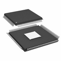
AD9957BSVZ Analog Devices Inc, AD9957BSVZ Datasheet - Page 21

AD9957BSVZ
Manufacturer Part Number
AD9957BSVZ
Description
IC DDS 1GSPS 14BIT IQ 100TQFP
Manufacturer
Analog Devices Inc
Datasheet
1.AD9957BSVZ-REEL.pdf
(64 pages)
Specifications of AD9957BSVZ
Resolution (bits)
14 b
Master Fclk
1GHz
Tuning Word Width (bits)
32 b
Voltage - Supply
1.8V, 3.3V
Operating Temperature
-40°C ~ 85°C
Mounting Type
Surface Mount
Package / Case
100-TQFP Exposed Pad, 100-eTQFP, 100-HTQFP, 100-VQFP
Frequency Range
60MHz To 1GHz
Rf Type
Quadrature
Supply Voltage Range
1.71V To 1.89V, 3.135V To 3.465
Rf Ic Case Style
TQFP
No. Of Pins
100
Operating Temperature Range
-40°C To +85°C
Operating Temperature (max)
85C
Operating Temperature (min)
-40C
Pin Count
100
Mounting
Surface Mount
Case Height
1mm
Screening Level
Industrial
Lead Free Status / RoHS Status
Lead free / RoHS Compliant
For Use With
AD9957/PCBZ - BOARD EVAL AD9957 QUADRATURE MOD
Lead Free Status / Rohs Status
Compliant
Available stocks
Company
Part Number
Manufacturer
Quantity
Price
Company:
Part Number:
AD9957BSVZ
Manufacturer:
AD
Quantity:
1 200
Company:
Part Number:
AD9957BSVZ
Manufacturer:
Analog Devices Inc
Quantity:
10 000
Part Number:
AD9957BSVZ
Manufacturer:
ADI/亚德诺
Quantity:
20 000
Company:
Part Number:
AD9957BSVZ-REEL
Manufacturer:
Analog Devices Inc
Quantity:
10 000
Part Number:
AD9957BSVZ-REEL
Manufacturer:
ADI/亚德诺
Quantity:
20 000
SIGNAL PROCESSING
For a better understanding of the operation of the AD9957, it
is helpful to follow the signal path in quadrature modulation
mode from the parallel data port to the output of the DAC,
examining the function of each block (see Figure 26).
The internal system clock (SYSCLK) signal that generates from
the timing source provided to the REF_CLK pins provides all
timing within the AD9957.
PARALLEL DATA CLOCK (PDCLK)
The AD9957 generates a signal on the PDCLK pin, which is a
clock signal that runs at the sample rate of the parallel data port.
PDCLK serves as a data clock for the parallel port in QDUC
and interpolating DAC modes; in BFI mode, it is a bit clock.
Normally, the device uses the rising edges on PDCLK to latch
the user-supplied data into the data port. Alternatively, the
PDCLK Invert bit selects the falling edges as the active edges.
Furthermore, the PDCLK enable bit is used to switch off the
PDCLK signal. Even when the output signal is turned off via the
PDCLK enable bit, PDCLK continues to operate internally. The
device uses PDCLK internally to capture parallel data. Note that
PDCLK is Logic 0 when disabled.
In QDUC mode, the AD9957 expects alternating I- and Q-
data-words at the parallel port (see Figure 31). Each active edge
of PDCLK captures one 18-bit word; therefore, there are two
PDCLK cycles per I/Q pair. In BFI mode, the AD9957 expects
two serial bit streams, each segmented into 16-bit words with
PDCLK indicating each new bit. In either case, the output clock
rate is f
In QDUC applications that require a consistent timing relation-
ship between the internal SYSCLK signal and the PDCLK signal,
the PDCLK rate control bit is used to slightly alter the operation
of PDCLK. When this bit is set, the PDCLK rate is reduced by
a factor of two. This causes rising edges on PDCLK to latch
incoming I-words and falling edges to latch incoming Q-words.
Again, the edge polarity assignment is reversible via the PDCLK
Invert bit.
PDCLK
as explained in the Input Data Assembler section.
Rev. B | Page 21 of 64
TRANSMIT ENABLE PIN (TxENABLE)
The AD9957 accepts a user-generated signal applied to the
TxENABLE pin that gates the user supplied data. Polarity of
the TxENABLE pin is set using the TxENABLE invert bit (see
the Register Map section for details). When TxENABLE is true,
the device latches data into the device on the expected edge of
PDCLK (based on the PDCLK invert bit). When TxENABLE
is false, the device ignores the data supplied to the port, even
though the PDCLK may continue to operate. Furthermore,
when the TxENABLE pin is held false, then the device either
forces the 18-bit data-words to Logic 0s, or it retains the last
value present on the data port prior to TxENABLE switching
to the false state (see the data assembler hold last value bit in
the Register Map section).
Alternatively, rather than operating the TxENABLE pin as a
gate for framing bursts of data, it can be driven with a clock
signal operating at the parallel port data rate. When driven by
a clock signal, the transition from the false to true state must
meet the required setup and hold times on each cycle to ensure
proper operation.
In QDUC mode, on the false-to-true edge of TxENABLE, the
device is ready to receive the first I-word. The first I-word is
latched into the device coincident with the active edge of PDCLK.
The next active edge of PDCLK latches in a Q-word, and so on,
until TxENABLE is returned to a static false state. The user may
reverse the ordering of the I- and Q-words via the Q-First Data
Pairing bit. Furthermore, the user must ensure that an even
number of data words are delivered to the device as it must
capture both an I- and a Q-word before the data is processed
along the signal chain.
In interpolating DAC mode, TxENABLE operation is similar to
QDUC mode, but without the need for I/Q data pairing; the
even-number-of-PDCLK-cycles rule does not apply.
In BFI mode, operation of the TxENABLE pin is similar except
that instead of the false-to-true edge marking the first I-word,
it marks the first I and Q bits in a serial frame. The user must
ensure that all 16-bits of a serial frame are delivered because the
device must capture a full 16-bit I- and Q-word before the data
is processed along the signal chain.
The timing relationships between TxENABLE, PDCLK, and
DATA are shown in Figure 30, Figure 31, and Figure 32.
AD9957


