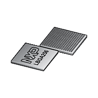
LPC1850FET256 NXP Semiconductors, LPC1850FET256 Datasheet - Page 69

LPC1850FET256
Manufacturer Part Number
LPC1850FET256
Description
The LPC1850FET256 is a high-performance, cost-effective Cortex-M3 microcontroller featuring 200 kB of SRAM, and advanced peripherals including Ethernet, High Speed USB 2
Manufacturer
NXP Semiconductors
Datasheet
1.LPC1810FBD144.pdf
(157 pages)
Available stocks
Company
Part Number
Manufacturer
Quantity
Price
Company:
Part Number:
LPC1850FET256
Manufacturer:
NXP
Quantity:
1 000
Part Number:
LPC1850FET256
Manufacturer:
NXP/恩智浦
Quantity:
20 000
Company:
Part Number:
LPC1850FET256,551
Manufacturer:
NXP Semiconductors
Quantity:
10 000
Part Number:
LPC1850FET256,551
Manufacturer:
NXP/恩智浦
Quantity:
20 000
NXP Semiconductors
LPC1850_30_20_10
Preliminary data sheet
7.4.2 Interrupt sources
7.6.1 Features
7.5 Event router
7.6 Global Input Multiplexer Array (GIMA)
7.7 System Tick timer (SysTick)
7.8 On-chip static RAM
Each peripheral device has one interrupt line connected to the NVIC but may have several
interrupt flags. Individual interrupt flags may also represent more than one interrupt
source.
The event router combines various internal signals, interrupts, and the external interrupt
pins (WAKEUP[3:0]) to create an interrupt in the NVIC if enabled and to create a wake-up
signal to the ARM core and the CCU for waking up from Sleep, Deep-sleep, Power-down,
and Deep power-down modes. Individual events can be configured as edge or level
sensitive and can be enabled or disabled in the event router. The event router can be
battery powered.
The following events if enabled in the event router can create a wake-up signal and/or an
interrupt:
The GIMA allows to route signals to event-driven peripheral targets like the SCT, timers,
event router, or the ADCs.
The ARM Cortex-M3 includes a system tick timer (SYSTICK) that is intended to generate
a dedicated SYSTICK exception at a 10 ms interval.
The LPC1850/30/20/10 support up to 200 kB SRAM with separate bus master access for
higher throughput and individual power control for low power operation.
•
•
•
•
•
•
•
•
•
•
External pins WAKEUP0/1/2/3 and RESET
Alarm timer, RTC, WWDT, BOD interrupts
C_CAN and QEI interrupts
Ethernet, USB0, USB1 signals
Selected outputs of combined timers (SCT and timer0/1/3)
Single selection of a source.
Signal inversion.
Can capture a pulse if the input event source is faster than the target clock.
Synchronization of input event and target clock.
Single-cycle pulse generation for target.
All information provided in this document is subject to legal disclaimers.
Rev. 3.1 — 15 December 2011
32-bit ARM Cortex-M3 microcontroller
LPC1850/30/20/10
© NXP B.V. 2011. All rights reserved.
69 of 157


