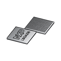
LPC1850FET256 NXP Semiconductors, LPC1850FET256 Datasheet - Page 70

LPC1850FET256
Manufacturer Part Number
LPC1850FET256
Description
The LPC1850FET256 is a high-performance, cost-effective Cortex-M3 microcontroller featuring 200 kB of SRAM, and advanced peripherals including Ethernet, High Speed USB 2
Manufacturer
NXP Semiconductors
Datasheet
1.LPC1810FBD144.pdf
(157 pages)
Available stocks
Company
Part Number
Manufacturer
Quantity
Price
Company:
Part Number:
LPC1850FET256
Manufacturer:
NXP
Quantity:
1 000
Part Number:
LPC1850FET256
Manufacturer:
NXP/恩智浦
Quantity:
20 000
Company:
Part Number:
LPC1850FET256,551
Manufacturer:
NXP Semiconductors
Quantity:
10 000
Part Number:
LPC1850FET256,551
Manufacturer:
NXP/恩智浦
Quantity:
20 000
NXP Semiconductors
Table 4.
LPC1850_30_20_10
Preliminary data sheet
Boot mode BOOT_SRC
Pin state
USART0
SPIFI
EMC 8-bit
EMC 16-bit
EMC 32-bit
USB0
Boot mode when OTP BOOT_SRC bits are programmed
bit 3
0
0
0
0
0
0
0
7.8.1 ISP (In-System Programming) mode
7.9 Boot ROM
In-System Programming (ISP) is programming or reprogramming the on-chip SRAM
memory, using the boot loader software and the USART0 serial port. ISP can be used
when the part resides in the end-user board. ISP allows to load data into on-chip SRAM
and execute code from on-chip SRAM.
The internal ROM memory is used to store the boot code of the LPC1850/30/20/10. After
a reset, the ARM processor will start its code execution from this memory.
The boot ROM memory includes the following features:
AES capable parts also support:
Several boot modes are available depending on the values of the OTP bits BOOT_SRC. If
the OTP memory is not programmed or the BOOT_SRC bits are all zero, the boot mode is
determined by the states of the boot pins P2_9, P2_8, P1_2, and P1_1.
•
•
•
•
•
•
•
BOOT_SRC
bit 2
0
0
0
0
1
1
1
ROM memory size is 64 kB.
Supports booting from USART interfaces and external static memory such as NOR
flash, and SPI flash.
Includes API for OTP programming.
Includes a flexible USB device stack that supports Human Interface Device (HID),
Mass Storage Class (MSC), and Device Firmware Upgrade (DFU) drivers.
CMAC authentication on the boot image.
Secure booting from an encrypted image. In development mode booting from a plain
text image is possible. Development mode is terminated by programming the AES
key.
API for AES programming.
All information provided in this document is subject to legal disclaimers.
BOOT_SRC
bit 1
0
0
1
1
0
0
1
Rev. 3.1 — 15 December 2011
BOOT_SRC
bit 0
0
1
0
1
0
1
0
Description
Boot source is defined by the reset state of P1_1,
P1_2, P2_8, and P2_9 pins. See
Boot from device connected to USART0 using pins
P2_0 and P2_1.
Boot from Quad SPI flash connected to the SPIFI
interface using pins P3_3 to P3_8.
Boot from external static memory (such as NOR
flash) using CS0 and an 8-bit data bus.
Boot from external static memory (such as NOR
flash) using CS0 and a 16-bit data bus.
Boot from external static memory (such as NOR
flash) using CS0 and a 32-bit data bus.
Boot from USB0.
32-bit ARM Cortex-M3 microcontroller
LPC1850/30/20/10
© NXP B.V. 2011. All rights reserved.
Table
5.
70 of 157


