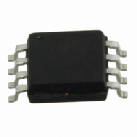
W25Q32BVSSIG Winbond Electronics, W25Q32BVSSIG Datasheet - Page 25

W25Q32BVSSIG
Manufacturer Part Number
W25Q32BVSSIG
Description
IC SPI FLASH 32MBIT 8SOIC
Manufacturer
Winbond Electronics
Datasheet
1.W25Q32BVZPIG.pdf
(79 pages)
Specifications of W25Q32BVSSIG
Format - Memory
FLASH
Memory Type
FLASH
Memory Size
32M (4M x 8)
Speed
104MHz
Interface
SPI Serial
Voltage - Supply
2.7 V ~ 3.6 V
Operating Temperature
-40°C ~ 85°C
Package / Case
8-SOIC (5.3mm Width), 8-SOP, 8-SOEIAJ
Lead Free Status / RoHS Status
Lead free / RoHS Compliant
Available stocks
Company
Part Number
Manufacturer
Quantity
Price
Company:
Part Number:
W25Q32BVSSIG
Manufacturer:
Winbond
Quantity:
1 000
Company:
Part Number:
W25Q32BVSSIG
Manufacturer:
WINBOND
Quantity:
9 310
Company:
Part Number:
W25Q32BVSSIG
Manufacturer:
Winbond
Quantity:
6 600
Part Number:
W25Q32BVSSIG
Manufacturer:
WINBOND/华邦
Quantity:
20 000
7.2.8 Read Status Register-1 (05h) and Read Status Register-2 (35h)
The Read Status Register instructions allow the 8-bit Status Registers to be read. The instruction is
entered by driving /CS low and shifting the instruction code “05h” for Status Register-1 or “35h” for Status
Register-2 into the DI pin on the rising edge of CLK. The status register bits are then shifted out on the DO
pin at the falling edge of CLK with most significant bit (MSB) first as shown in Figure 7. The Status
Register bits are shown in Figure 3a and 3b and include the BUSY, WEL, BP2-BP0, TB, SEC, SRP0,
SRP1, QE, LB[3:1], CMP and SUS bits (see Status Register section earlier in this datasheet).
The Read Status Register instruction may be used at any time, even while a Program, Erase or Write
Status Register cycle is in progress. This allows the BUSY status bit to be checked to determine when the
cycle is complete and if the device can accept another instruction. The Status Register can be read
continuously, as shown in Figure 7. The instruction is completed by driving /CS high.
7.2.9 Write Status Register (01h)
The Write Status Register instruction allows the Status Register to be written. Only non-volatile Status
Register bits SRP0, SEC, TB, BP2, BP1, BP0 (bits 7 thru 2 of Status Register-1) and CMP, LB3, LB2,
LB1, QE, SRP1 (bits 14 thru 8 of Status Register-2) can be written to. All other Status Register bit
locations are read-only and will not be affected by the Write Status Register instruction. LB[3:1] are non-
volatile OTP bits, once it is set to 1, it can not be cleared to 0. The Status Register bits are shown in
Figure 3 and described in 7.1.
To write non-volatile Status Register bits, a standard Write Enable (06h) instruction must previously have
been executed for the device to accept the Write Status Register Instruction (Status Register bit WEL
must equal 1). Once write enabled, the instruction is entered by driving /CS low, sending the instruction
code “01h”, and then writing the status register data byte as illustrated in Figure 8.
To write volatile Status Register bits, a Write Enable for Volatile Status Register (50h) instruction must
have been executed prior to the Write Status Register instruction (Status Register bit WEL remains 0).
However, SRP1 and LB3, LB2, LB1 can not be changed from “1” to “0” because of the OTP protection for
these bits. Upon power off, the volatile Status Register bit values will be lost, and the non-volatile Status
Register bit values will be restored when power on again.
(IO
(IO
CLK
/CS
DO
DI
0
1
)
)
Mode 3
Mode 0
*
= MSB
0
1
Instruction (05h or 35h)
High Impedance
2
Figure 7. Read Status Register Instruction Sequence Diagram
3
4
5
6
7
*
7
8
6
Status Register 1 or 2 out
9
- 25 -
5
10
4
11
3
12
2
13
1
14
Publication Release Date: April 01, 2011
0
15
*
7
16
6
Status Register 1 or 2 out
17
5
18
4
19
W25Q32BV
3
20
2
21
1
22
Revision F
0
23
7


