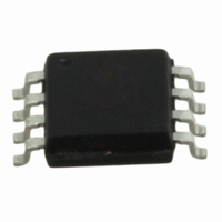
W25Q32BVSSIG Winbond Electronics, W25Q32BVSSIG Datasheet - Page 60

W25Q32BVSSIG
Manufacturer Part Number
W25Q32BVSSIG
Description
IC SPI FLASH 32MBIT 8SOIC
Manufacturer
Winbond Electronics
Datasheet
1.W25Q32BVZPIG.pdf
(79 pages)
Specifications of W25Q32BVSSIG
Format - Memory
FLASH
Memory Type
FLASH
Memory Size
32M (4M x 8)
Speed
104MHz
Interface
SPI Serial
Voltage - Supply
2.7 V ~ 3.6 V
Operating Temperature
-40°C ~ 85°C
Package / Case
8-SOIC (5.3mm Width), 8-SOP, 8-SOEIAJ
Lead Free Status / RoHS Status
Lead free / RoHS Compliant
Available stocks
Company
Part Number
Manufacturer
Quantity
Price
Company:
Part Number:
W25Q32BVSSIG
Manufacturer:
Winbond
Quantity:
1 000
Company:
Part Number:
W25Q32BVSSIG
Manufacturer:
WINBOND
Quantity:
9 310
Company:
Part Number:
W25Q32BVSSIG
Manufacturer:
Winbond
Quantity:
6 600
Part Number:
W25Q32BVSSIG
Manufacturer:
WINBOND/华邦
Quantity:
20 000
7.2.37 Erase Security Registers (44h)
The W25Q32BV offers three 256-byte Security Registers which can be erased and programmed
individually. These registers may be used by the system manufacturers to store security and other
important information separately from the main memory array.
The Erase Security Register instruction is similar to the Sector Erase instruction. A Write Enable
instruction must be executed before the device will accept the Erase Security Register Instruction (Status
Register bit WEL must equal 1). The instruction is initiated by driving the /CS pin low and shifting the
instruction code “44h” followed by a 24-bit address (A23-A0) to erase one of the three security registers.
The Erase Security Register instruction sequence is shown in Figure 35. The /CS pin must be driven high
after the eighth bit of the last byte has been latched. If this is not done the instruction will not be executed.
After /CS is driven high, the self-timed Erase Security Register operation will commence for a time
duration of t
Status Register instruction may still be accessed for checking the status of the BUSY bit. The BUSY bit is
a 1 during the erase cycle and becomes a 0 when the cycle is finished and the device is ready to accept
other instructions again. After the Erase Security Register cycle has finished the Write Enable Latch
(WEL) bit in the Status Register is cleared to 0. The Security Register Lock Bits LB[3:1] in the Status
Register-2 can be used to OTP protect the security registers. Once a lock bit is set to 1, the corresponding
security register will be permanently locked, Erase Security Register instruction to that register will be
ignored (See 7.1.9 for detail descriptions).
Security Register #1
Security Register #2
Security Register #3
SE
(IO
(IO
CLK
/CS
DO
DI
0
1
(See AC Characteristics). While the Erase Security Register cycle is in progress, the Read
)
)
ADDRESS
Mode 3
Mode 0
*
= MSB
Figure 35. Erase Security Registers Instruction Sequence
0
1
Instruction (44h)
2
A23-16
00h
00h
00h
3
4
High Impedance
5
- 60 -
6
A15-12
0 0 0 1
0 0 1 0
0 0 1 1
7
23
*
8
22
24-Bit Address
9
0 0 0 0
0 0 0 0
0 0 0 0
A11-8
2
29
1
30
0
31
W25Q32BV
Don’t Care
Don’t Care
Don’t Care
Mode 3
Mode 0
A7-0


