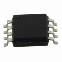
W25Q32BVSSIG Winbond Electronics, W25Q32BVSSIG Datasheet - Page 62

W25Q32BVSSIG
Manufacturer Part Number
W25Q32BVSSIG
Description
IC SPI FLASH 32MBIT 8SOIC
Manufacturer
Winbond Electronics
Datasheet
1.W25Q32BVZPIG.pdf
(79 pages)
Specifications of W25Q32BVSSIG
Format - Memory
FLASH
Memory Type
FLASH
Memory Size
32M (4M x 8)
Speed
104MHz
Interface
SPI Serial
Voltage - Supply
2.7 V ~ 3.6 V
Operating Temperature
-40°C ~ 85°C
Package / Case
8-SOIC (5.3mm Width), 8-SOP, 8-SOEIAJ
Lead Free Status / RoHS Status
Lead free / RoHS Compliant
Available stocks
Company
Part Number
Manufacturer
Quantity
Price
Company:
Part Number:
W25Q32BVSSIG
Manufacturer:
Winbond
Quantity:
1 000
Company:
Part Number:
W25Q32BVSSIG
Manufacturer:
WINBOND
Quantity:
9 310
Company:
Part Number:
W25Q32BVSSIG
Manufacturer:
Winbond
Quantity:
6 600
Part Number:
W25Q32BVSSIG
Manufacturer:
WINBOND/华邦
Quantity:
20 000
7.2.39 Read Security Registers (48h)
The Read Security Register instruction is similar to the Fast Read instruction and allows one or more data
bytes to be sequentially read from one of the three security registers. The instruction is initiated by driving
the /CS pin low and then shifting the instruction code “48h” followed by a 24-bit address (A23-A0) and
eight “dummy” clocks into the DI pin. The code and address bits are latched on the rising edge of the CLK
pin. After the address is received, the data byte of the addressed memory location will be shifted out on
the DO pin at the falling edge of CLK with most significant bit (MSB) first. The byte address is
automatically incremented to the next byte address after each byte of data is shifted out. Once the byte
address reaches the last byte of the register (byte FFh), it will reset to 00h, the first byte of the register,
and continue to increment. The instruction is completed by driving /CS high. The Read Security Register
instruction sequence is shown in Figure 37. If a Read Security Register instruction is issued while an
Erase, Program or Write cycle is in process (BUSY=1) the instruction is ignored and will not have any
effects on the current cycle. The Read Security Register instruction allows clock rates from D.C. to a
maximum of F
CLK
(IO
(IO
CLK
(IO
(IO
/CS
/CS
DO
DO
DI
DI
0
1
0
1
)
)
)
)
Mode 3
Mode 0
0
31
*
Security Register #1
Security Register #2
Security Register #3
7
= MSB
32
R
ADDRESS
(see AC Electrical Characteristics).
6
33
High Impedance
0
5
34
Dummy Byte
1
4
35
Instruction (48h)
2
3
36
3
Figure 37. Read Security Registers Instruction Sequence
2
37
4
High Impedance
1
38
5
0
39
6
A23-16
*
7
00h
00h
00h
40
7
6
23
41
*
8
5
22
42
- 62 -
9
Data Out 1
4
21
43
10
24-Bit Address
3
A15-12
0 0 0 1
0 0 1 0
0 0 1 1
44
2
45
3
28
1
46
2
29
0
47
1
30
*
7
48
0
31
0 0 0 0
0 0 0 0
0 0 0 0
A11-8
6
49
5
50
Data Out 2
4
51
W25Q32BV
3
Byte Address
Byte Address
Byte Address
52
2
A7-0
53
1
54
0
55
7


