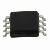
W25Q32BVSSIG Winbond Electronics, W25Q32BVSSIG Datasheet - Page 49

W25Q32BVSSIG
Manufacturer Part Number
W25Q32BVSSIG
Description
IC SPI FLASH 32MBIT 8SOIC
Manufacturer
Winbond Electronics
Datasheet
1.W25Q32BVZPIG.pdf
(79 pages)
Specifications of W25Q32BVSSIG
Format - Memory
FLASH
Memory Type
FLASH
Memory Size
32M (4M x 8)
Speed
104MHz
Interface
SPI Serial
Voltage - Supply
2.7 V ~ 3.6 V
Operating Temperature
-40°C ~ 85°C
Package / Case
8-SOIC (5.3mm Width), 8-SOP, 8-SOEIAJ
Lead Free Status / RoHS Status
Lead free / RoHS Compliant
Available stocks
Company
Part Number
Manufacturer
Quantity
Price
Company:
Part Number:
W25Q32BVSSIG
Manufacturer:
Winbond
Quantity:
1 000
Company:
Part Number:
W25Q32BVSSIG
Manufacturer:
WINBOND
Quantity:
9 310
Company:
Part Number:
W25Q32BVSSIG
Manufacturer:
Winbond
Quantity:
6 600
Part Number:
W25Q32BVSSIG
Manufacturer:
WINBOND/华邦
Quantity:
20 000
7.2.29 Power-down (B9h)
Although the standby current during normal operation is relatively low, standby current can be further
reduced with the Power-down instruction. The lower power consumption makes the Power-down
instruction especially useful for battery powered applications (See ICC1 and ICC2 in AC Characteristics).
The instruction is initiated by driving the /CS pin low and shifting the instruction code “B9h” as shown in
Figure 27.
The /CS pin must be driven high after the eighth bit has been latched. If this is not done the Power-down
instruction will not be executed. After /CS is driven high, the power-down state will entered within the time
duration of t
down / Device ID instruction, which restores the device to normal operation, will be recognized. All other
instructions are ignored. This includes the Read Status Register instruction, which is always available
during normal operation. Ignoring all but one instruction makes the Power Down state a useful condition
for securing maximum write protection. The device always powers-up in the normal operation with the
standby current of ICC1.
(IO
CLK
/CS
DI
0
)
DP
Mode 3
Mode 0
(See AC Characteristics). While in the power-down state only the Release from Power-
0
Figure 27. Deep Power-down Instruction Sequence Diagram
1
Instruction (B9h)
2
3
4
5
6
- 49 -
7
Stand-by current
Publication Release Date: April 01, 2011
tDP
Power-down current
Mode 3
Mode 0
W25Q32BV
Revision F


