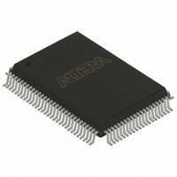
EPC8QI100 Altera, EPC8QI100 Datasheet - Page 22

EPC8QI100
Manufacturer Part Number
EPC8QI100
Description
IC CONFIG DEVICE 8MBIT 100-PQFP
Manufacturer
Altera
Series
EPCr
Datasheet
1.EPC8QC100.pdf
(34 pages)
Specifications of EPC8QI100
Programmable Type
In System Programmable
Memory Size
8Mb
Voltage - Supply
3 V ~ 3.6 V
Operating Temperature
-40°C ~ 85°C
Package / Case
100-MQFP, 100-PQFP
Lead Free Status / RoHS Status
Contains lead / RoHS non-compliant
Other names
544-1239
Available stocks
Company
Part Number
Manufacturer
Quantity
Price
Company:
Part Number:
EPC8QI100
Manufacturer:
ALTERA
Quantity:
10
Company:
Part Number:
EPC8QI100
Manufacturer:
ALTERA
Quantity:
710
Part Number:
EPC8QI100
Manufacturer:
ALTERA
Quantity:
20 000
Company:
Part Number:
EPC8QI100N
Manufacturer:
ALTERA
Quantity:
1 500
Company:
Part Number:
EPC8QI100N
Manufacturer:
ALTERA21
Quantity:
444
1–22
Table 1–8. Configuration Interface Pins (Part 2 of 2)
Table 1–9. External Flash Interface Pins (Part 1 of 3)
Configuration Handbook (Complete Two-Volume Set)
nCS
nINIT_CONF
OE
A[20..0]
DQ[15..0]
CE#
Pin Name
Pin Name
Open-Drain Output
Bidirectional
Bidirectional
Open-Drain
Pin Type
Pin Type
Input
Input
Input
These pins are the address input to the flash memory for read and write
operations. The addresses are internally latched during a write cycle.
When the external flash interface is not used, leave these pins floating (with a few
exceptions(1)). These flash address, data, and control pins are internally
connected to the configuration controller.
In the 100-pin PQFP package, four address pins (A0, A1, A15, A16) are not
internally connected to the controller. These loop-back connections must be made
on the board between the C-A[] and F-A[] pins even when not using the
external flash interface. All other address pins are connected internal to the
package.
All address pins are connected internally in the 88-pin UFBGA package.
Pin A20 in EPC16 devices, pins A20 and A19 in EPC8 devices, and pins A20,
A19, and A18 in EPC4 devices are no-connects. These pins should be left
floating on the board.
This is the flash data bus interface between the flash memory and the controller.
The controller or an external source drives DQ[15..0] during the flash
command and the data write bus cycles. During the data read cycle, the flash
memory drives the DQ[15..0] to the controller or external device.
Leave these pins floating on the board when the external flash interface is not
used.
Active low flash input pin that activates the flash memory when asserted. When it
is high, it deselects the device and reduces power consumption to standby levels.
This flash input pin is internally connected to the controller.
Leave this pin floating on the board when the external flash interface is not used.
The nCS pin is an input to the enhanced configuration device and is connected to
the FPGA’s CONF_DONE signal for error detection after all configuration data is
transmitted to the FPGA. The FPGA will always drive nCS and OE low when
nCONFIG is asserted. This pin contains a programmable internal weak pull-up
resistor of 6K that can be disabled/enabled in the Quartus II software through
the Disable nCS and OE pull-ups on configuration device option.
The nINIT_CONF pin can be connected to the nCONFIG pin on the FPGA to
initiate configuration from the enhanced configuration device via a private JTAG
instruction. This pin contains an internal weak pull-up resistor of 6K that is
always active. The INIT_CONF pin does not need to be connected if its
functionality is not used. If n
to V
This pin is driven low when POR is not complete. A user-selectable 2-ms or
100-ms counter holds off the release of OE during initial power up to permit
voltage levels to stabilize. POR time can be extended by externally holding OE
low. OE is connected to the FPGA nSTATUS signal. After the enhanced
configuration device controller releases OE, it waits for the nSTATUS-OE line to
go high before starting the FPGA configuration process. This pin contains a
programmable internal weak pull-up resistor of 6K that can be
disabled/enabled in the Quartus II software through the Disable nCS and OE
pull
CC
- ups on configuration device option.
either directly or through a pull-up resistor.
Chapter 1: Enhanced Configuration Devices (EPC4, EPC8, and EPC16) Data Sheet
INIT _CONF is not used, nCONFIG must be pulled
Description
Description
© December 2009 Altera Corporation
Pin Description


