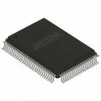
EPC8QI100 Altera, EPC8QI100 Datasheet - Page 23

EPC8QI100
Manufacturer Part Number
EPC8QI100
Description
IC CONFIG DEVICE 8MBIT 100-PQFP
Manufacturer
Altera
Series
EPCr
Datasheet
1.EPC8QC100.pdf
(34 pages)
Specifications of EPC8QI100
Programmable Type
In System Programmable
Memory Size
8Mb
Voltage - Supply
3 V ~ 3.6 V
Operating Temperature
-40°C ~ 85°C
Package / Case
100-MQFP, 100-PQFP
Lead Free Status / RoHS Status
Contains lead / RoHS non-compliant
Other names
544-1239
Available stocks
Company
Part Number
Manufacturer
Quantity
Price
Company:
Part Number:
EPC8QI100
Manufacturer:
ALTERA
Quantity:
10
Company:
Part Number:
EPC8QI100
Manufacturer:
ALTERA
Quantity:
710
Part Number:
EPC8QI100
Manufacturer:
ALTERA
Quantity:
20 000
Company:
Part Number:
EPC8QI100N
Manufacturer:
ALTERA
Quantity:
1 500
Company:
Part Number:
EPC8QI100N
Manufacturer:
ALTERA21
Quantity:
444
Chapter 1: Enhanced Configuration Devices (EPC4, EPC8, and EPC16) Data Sheet
Pin Description
Table 1–9. External Flash Interface Pins (Part 2 of 3)
© December 2009 Altera Corporation
RP#
OE#
WE#
WP#
V
RY/BY#
CCW
Pin Name
(1)
(1)
Open-Drain Output
Pin Type
Supply
Input
Input
Input
Input
Active low flash input pin that resets the flash when asserted. When high, it
enables normal operation. When low, it inhibits write operation to the flash
memory, which provides data protection during power transitions.
This flash input is not internally connected to the controller. Hence, an external
loop-back connection between C-RP# and F-RP# must be made on the board
even when you are not using the external flash interface.
When using the external flash interface, connect the external device to the RP#
pin with the loop back. Always tri-state RP# when the flash is not in use.
Active-low flash-control input that is asserted by the controller or external device
during flash read cycles. When asserted, it enables the drivers of the flash output
pins.
Leave this pin floating on the board when the external flash interface is not used.
Active-low flash-write strobe asserted by the controller or external device during
flash write cycles. When asserted, it controls writes to the flash memory. In the
flash memory, addresses and data are latched on the rising edge of the WE#
pulse.
This flash input is not internally connected to the controller. Hence, an external
loop-back connection between C-WE# and F-WE# must be made on the board
even when you are not using the external flash interface.
When using the external flash interface, connect the external device to the WE#
pin with the loop back.
Usually tied to V
because it could cause contention.
Connection to V
to allow programming of the flash-bottom boot block, which is required when
programming the device using the Quartus II software.
This pin should be connected to V
used.
Block erase, full-chip erase, word write, or lock-bit configuration power supply.
Connect this pin to the 3.3-V V
flash interface.
Flash asserts this pin when a write or erase operation is complete. This pin is not
connected to the controller. RY/BY# is only available in Sharp flash-based EPC8
and EPC16.
Leave this pin floating when the external flash interface is not used.
(2)
CC
CC
is recommended for faster block erase/programming times and
or ground on the board. The controller does not drive this pin
CC
supply, even when you are not using the external
CC
Description
even when the external flash interface is not
Configuration Handbook (Complete Two-Volume Set)
1–23


