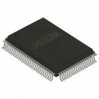
EPC8QI100 Altera, EPC8QI100 Datasheet - Page 9

EPC8QI100
Manufacturer Part Number
EPC8QI100
Description
IC CONFIG DEVICE 8MBIT 100-PQFP
Manufacturer
Altera
Series
EPCr
Datasheet
1.EPC8QC100.pdf
(34 pages)
Specifications of EPC8QI100
Programmable Type
In System Programmable
Memory Size
8Mb
Voltage - Supply
3 V ~ 3.6 V
Operating Temperature
-40°C ~ 85°C
Package / Case
100-MQFP, 100-PQFP
Lead Free Status / RoHS Status
Contains lead / RoHS non-compliant
Other names
544-1239
Available stocks
Company
Part Number
Manufacturer
Quantity
Price
Company:
Part Number:
EPC8QI100
Manufacturer:
ALTERA
Quantity:
10
Company:
Part Number:
EPC8QI100
Manufacturer:
ALTERA
Quantity:
710
Part Number:
EPC8QI100
Manufacturer:
ALTERA
Quantity:
20 000
Company:
Part Number:
EPC8QI100N
Manufacturer:
ALTERA
Quantity:
1 500
Company:
Part Number:
EPC8QI100N
Manufacturer:
ALTERA21
Quantity:
444
Chapter 1: Enhanced Configuration Devices (EPC4, EPC8, and EPC16) Data Sheet
Functional Description
© December 2009 Altera Corporation
Configuration Signals
Table 1–4
configuration device and Altera FPGAs.
Table 1–4. Configuration Signals
Fast Passive Parallel Configuration
Stratix series and APEX II devices can be configured using the enhanced
configuration device in FPP mode. In this mode, the enhanced configuration device
sends a byte of data on the DATA[7..0] pins, which connect to the DATA[7..0]
input pins of the FPGA, per DCLK cycle. Stratix series and APEX II FPGAs receive
byte-wide configuration data per DCLK cycle.
configuration device in FPP configuration mode. In this figure, the external flash
interface is not used and hence most flash pins are left unconnected (with the few
noted exceptions). For specific details about configuration interface connections
including pull-up resistor values, supply voltages, and MSEL pin settings, refer to the
appropriate FPGA family chapter in the
DATA[]
DCLK
nINIT_CONF,
which
OE
nCS
Configuration
Device Pin
Enhanced
lists the configuration signal connections between the enhanced
DATA[]
DCLK
nCONFIG
nSTATUS
CONF_DONE
Altera FPGA Pin
Configuration data transmitted from the configuration
device to the FPGA, which is latched on the rising edge of
DCLK.
Configuration device generated clock used by the FPGA to
latch configuration data provided on the DATA[] pins.
Open-drain output from the configuration device that is
used to start FPGA reconfiguration using the initiate
configuration (INIT_CONF) JTAG instruction. This
connection is not needed if the INIT_CONF JTAG
instruction is not needed. If n
connected to nCONFIG, nCONFIG must be tied to V
either directly or through a pull-up resistor.
Open-drain bidirectional configuration status signal,
which is driven low by either device during POR and to
signal an error during configuration. Low pulse on OE
resets the enhanced configuration device controller.
Configuration done output signal driven by the FPGA.
Configuration
Figure 1–2
Configuration Handbook (Complete Two-Volume Set)
Handbook.
Description
shows the enhanced
INIT_CONF is not
CC
1–9


