EPC8QI100 Altera, EPC8QI100 Datasheet - Page 32
EPC8QI100
Manufacturer Part Number
EPC8QI100
Description
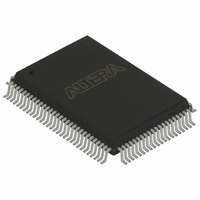
IC CONFIG DEVICE 8MBIT 100-PQFP
Manufacturer
Altera
Series
EPCr
Datasheet
1.EPC8QC100.pdf
(34 pages)
Specifications of EPC8QI100
Programmable Type
In System Programmable
Memory Size
8Mb
Voltage - Supply
3 V ~ 3.6 V
Operating Temperature
-40°C ~ 85°C
Package / Case
100-MQFP, 100-PQFP
Lead Free Status / RoHS Status
Contains lead / RoHS non-compliant
Other names
544-1239
Available stocks
Company
Part Number
Manufacturer
Quantity
Price
Company:

Part Number:
EPC8QI100
Manufacturer:
ALTERA
Quantity:
10
Company:
Part Number:
EPC8QI100
Manufacturer:
ALTERA
Quantity:
710
Part Number:
EPC8QI100
Manufacturer:
ALTERA
Quantity:
20 000
Company:
Part Number:
EPC8QI100N
Manufacturer:
ALTERA
Quantity:
1 500
Company:
Part Number:
EPC8QI100N
Manufacturer:
ALTERA21
Quantity:
444


1–32
Figure 1–8. PCB Routing for 88-Pin UFBGA Package
Notes to
(1) If the external flash interface feature is not used, then the flash pins should be left unconnected because they are internally connected to the
(2) F-RP# and F-WE# are pins on the flash die. C-RP# and C-WE# are pins on the controller die. C-WE# and F-WE# should be connected together
(3) WP# (write protection pin) should be connected to a high level (3.3 V) to be able to program the flash bottom boot block, which is required when
(4) RY/BY#
(5) Pin D3 is a NC pin for Intel Flash-based EPC16.
Package Layout Recommendation
Configuration Handbook (Complete Two-Volume Set)
controller unit. The only pins that need external connections are WP#, WE#, and RP#. If the flash is being used as an external memory source,
then the flash pins should be connected as outlined in the pin descriptions section.
on the PCB. F-RP# and C-RP# should also be connected together on the PCB.
programming the device using the Quartus II software.
Figure
is only available in Sharp flash-based enhanced configuration devices.
VCC
NC
OE
NC
1–8:
C-WE#
GND
VCC
TCK
TDO
TMS
nCS
TDI
(2)
Figure 1–8
this layout is on the Altera website.
Sharp flash-based EPC16 and EPC8 enhanced configuration devices in the 100-pin
PQFP packages have different package dimensions than other Altera 100-pin PQFP
devices (including the Micron flash-based EPC4, Intel flash-based EPC16, EPC8 and
EPC4).
configuration devices that allows for vertical migration between all devices. These
footprint dimensions are based on vendor-supplied package outline diagrams.
EXCLK
F-WE#
GND
A20
A16
A18
(2)
(5)
WP#
NC
Figure 1–9
(3)
shows the PCB routing for the 88-pin UFBGA package. The Gerber file for
RY/BY#
VCCW
F-RP#
A11
A17
NC
A8
(4)
(2)
A5
shows the 100-pin PQFP PCB footprint specifications for enhanced
CONF
PGM2
nINIT
TM1
A15
A10
A19
A7
A4
Chapter 1: Enhanced Configuration Devices (EPC4, EPC8, and EPC16) Data Sheet
(Note 1)
PORSEL
PGM1
DQ11
VCC
A14
A9
A6
A0
DQ15
DQ13
DQ12
VCC
DQ9
CE#
A13
A3
C-RP#
PGM0
DQ10
DQ6
DQ8
GND
A12
(2)
A2
DQ14
GND
VCC
DQ4
DQ2
DQ0
OE#
A1
DCLK
© December 2009 Altera Corporation
VCC
VCC
DQ7
DQ5
DQ3
DQ1
TM0
DATA7
DATA5
DATA4
DATA3
DATA2
DATA1
GND
GND
DATA0
DATA6
NC
NC
Package
Related parts for EPC8QI100
Image
Part Number
Description
Manufacturer
Datasheet
Request
R

Part Number:
Description:
IC CONFIG DEVICE 1MBIT 8-DIP
Manufacturer:
Altera
Datasheet:

Part Number:
Description:
IC CONFIG DEVICE 1.6MBIT 20-PLCC
Manufacturer:
Altera
Datasheet:
Part Number:
Description:
IC CONFIG DEVICE 1.6MBIT 20-PLCC
Manufacturer:
Altera
Datasheet:

Part Number:
Description:
IC CONFIG DEVICE 1.6MBIT 32-TQFP
Manufacturer:
Altera
Datasheet:
Part Number:
Description:
IC CONFIG DEVICE 1.6MBIT 32-TQFP
Manufacturer:
Altera
Datasheet:
Part Number:
Description:
IC CONFIG DEVICE 1.6MBIT 20-PLCC
Manufacturer:
Altera
Datasheet:
Part Number:
Description:
IC CONFIG DEVICE 1.6MBIT 20-PLCC
Manufacturer:
Altera
Datasheet:

Part Number:
Description:
IC CONFIG DEVICE 8MBIT 100-PQFP
Manufacturer:
Altera
Datasheet:
Part Number:
Description:
IC CONFIG DEVICE 1.6MBIT 32-TQFP
Manufacturer:
Altera
Datasheet:
Part Number:
Description:
IC CONFIG DEVICE 1.6MBIT 32-TQFP
Manufacturer:
Altera
Datasheet:
Part Number:
Description:
IC CONFIG DEVICE 16MBIT 100-PQFP
Manufacturer:
Altera
Datasheet:
Part Number:
Description:
IC CONFIG DEVICE 16MBIT 100-PQFP
Manufacturer:
Altera
Datasheet:
Part Number:
Description:
IC CONFIG DEVICE 16MBIT 100-PQFP
Manufacturer:
Altera
Datasheet:

Part Number:
Description:
IC CONFIG DEVICE 16MBIT 88-UBGA
Manufacturer:
Altera
Datasheet:
Part Number:
Description:
IC CONFIG DEVICE 212KBIT 20-PLCC
Manufacturer:
Altera
Datasheet: