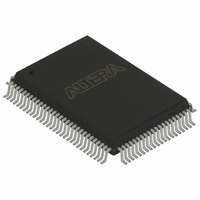
EPC8QI100 Altera, EPC8QI100 Datasheet - Page 8

EPC8QI100
Manufacturer Part Number
EPC8QI100
Description
IC CONFIG DEVICE 8MBIT 100-PQFP
Manufacturer
Altera
Series
EPCr
Datasheet
1.EPC8QC100.pdf
(34 pages)
Specifications of EPC8QI100
Programmable Type
In System Programmable
Memory Size
8Mb
Voltage - Supply
3 V ~ 3.6 V
Operating Temperature
-40°C ~ 85°C
Package / Case
100-MQFP, 100-PQFP
Lead Free Status / RoHS Status
Contains lead / RoHS non-compliant
Other names
544-1239
Available stocks
Company
Part Number
Manufacturer
Quantity
Price
Company:
Part Number:
EPC8QI100
Manufacturer:
ALTERA
Quantity:
10
Company:
Part Number:
EPC8QI100
Manufacturer:
ALTERA
Quantity:
710
Part Number:
EPC8QI100
Manufacturer:
ALTERA
Quantity:
20 000
Company:
Part Number:
EPC8QI100N
Manufacturer:
ALTERA
Quantity:
1 500
Company:
Part Number:
EPC8QI100N
Manufacturer:
ALTERA21
Quantity:
444
1–8
Configuration Handbook (Complete Two-Volume Set)
f
The function of the configuration unit is to transmit decompressed data to the FPGA,
depending on the configuration scheme. The enhanced configuration device supports
four concurrent configuration modes, with n = 1, 2, 4, or 8 (where n is the number of
bits that are sent per DCLK cycle on the DATA[n] lines). The value n = 1 corresponds
to the traditional PS configuration scheme. The values n = 2, 4, and 8 correspond to
concurrent configuration of 2, 4, or 8 different PS configuration chains, respectively.
Additionally, the FPGA can be configured in FPP mode, where eight bits of DATA are
clocked into the FPGA per DCLK cycle. Depending on the configuration bus width (n),
the circuit shifts uncompressed configuration data to the valid DATA[n] pins. Unused
DATA[] pins drive low.
In addition to transmitting configuration data to the FPGAs, the configuration circuit
is also responsible for pausing configuration whenever there is insufficient data
available for transmission. This occurs when the flash read bandwidth is lower than
the configuration write bandwidth. Configuration is paused by stopping the DCLK to
the FPGA, when waiting for data to be read from the flash or for data to be
decompressed. This technique is called “Pausing DCLK”.
The enhanced configuration device flash-memories feature a 90-ns access time
(approximately 10 MHz). Hence, the flash read bandwidth is limited to about 160
megabits per second (Mbps) (16-bit flash data bus, DQ[], at 10 MHz). However, the
configuration speeds supported by Altera FPGAs are much higher and translate to
high configuration write bandwidths. For instance, 100-MHz Stratix FPP
configuration requires data at the rate of 800 Mbps (8-bit DATA[] bus at 100 MHz).
This is much higher than the 160 Mbps the flash memory can support, and is the
limiting factor for configuration time. Compression increases the effective flash-read
bandwidth as the same amount of configuration data takes up less space in the flash
memory after compression. Since Stratix configuration data compression ratios are
approximately two, the effective read bandwidth doubles to about 320 Mbps.
Finally, the configuration controller also manages errors during configuration. A
CONF_DONE error occurs when the FPGA does not de-assert its CONF_DONE signal
within 64 DCLK cycles after the last bit of configuration data is transmitted. When a
CONF_DONE error is detected, the controller pulses the OE line low, which pulls
nSTATUS low and triggers another configuration cycle.
A cyclical redundancy check (CRC) error occurs when the FPGA detects corruption in
the configuration data. This corruption could be a result of noise coupling on the
board such as poor signal integrity on the configuration signals. When this error is
signaled by the FPGA (by driving the nSTATUS line low), the controller stops
configuration. If the Auto-Restart Configuration After Error option is enabled in the
FPGA, it releases its nSTATUS signal after a reset time-out period and the controller
attempts to reconfigure the FPGA.
After the FPGA configuration process is complete, the controller drives DCLK low and
the DATA[] pins high. Additionally, the controller tri-states its internal interface to the
flash memory, enables the weak internal pull-ups on the flash address and control
lines, and enables bus-keep circuits on flash data lines.
The following sections briefly describe the different configuration schemes supported
by the enhanced configuration device: FPP, PS, and concurrent configuration.
For detailed information about using these schemes to configure your Altera FPGA,
refer to the appropriate FPGA family chapter in the
Chapter 1: Enhanced Configuration Devices (EPC4, EPC8, and EPC16) Data Sheet
Configuration
© December 2009 Altera Corporation
Handbook.
Functional Description


