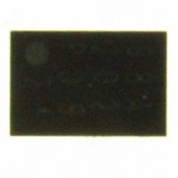
SE98ATP,547 NXP Semiconductors, SE98ATP,547 Datasheet - Page 13

SE98ATP,547
Manufacturer Part Number
SE98ATP,547
Description
IC TEMP SENSOR DDR 8-HWSON
Manufacturer
NXP Semiconductors
Datasheet
1.SE98ATP547.pdf
(43 pages)
Specifications of SE98ATP,547
Function
Temp Monitoring System (Sensor)
Topology
ADC (Sigma Delta), Register Bank
Sensor Type
Internal
Sensing Temperature
-40°C ~ 125°C
Output Type
I²C™/SMBus™
Output Alarm
Yes
Output Fan
Yes
Voltage - Supply
1.7 V ~ 3.6 V
Operating Temperature
-40°C ~ 125°C
Mounting Type
Surface Mount
Package / Case
8-WSON (Exposed Pad), 8-HWSON
Temperature Threshold
Programmable
Full Temp Accuracy
+/- 1 C
Digital Output - Bus Interface
2-Wire, SMBus, I2C
Digital Output - Number Of Bits
11
Supply Voltage (max)
3.6 V
Supply Voltage (min)
1.7 V
Description/function
DDR Memory Module Temperature Sensor
Maximum Operating Temperature
+ 125 C
Minimum Operating Temperature
- 40 C
Supply Current
250 uA
Lead Free Status / RoHS Status
Lead free / RoHS Compliant
Other names
568-4731-2
SE98ATP,147
SE98ATP,147
NXP Semiconductors
SE98A_4
Product data sheet
Fig 8.
SDA
SCL
START
S
A = ACK = Acknowledge bit. W = Write bit = 0. R = Read bit = 1.
SMBus/I
A6
1
7.9 SMBus/I
2
A5
C-bus write to the Pointer register
2
device address and write
The data registers in this device are selected by the Pointer register. At power-up, the
Pointer register is set to ‘00’, the location for the Capability register. The Pointer register
latches the last location it was set to. Each data register falls into one of three types of
user accessibility:
A ‘write’ to this device will always include the address byte and the pointer byte. A write to
any register other than the Pointer register requires two data bytes.
Reading this device can take place either of two ways:
The data byte has the most significant bit first. At the end of a read, this device can accept
either Acknowledge (ACK) or No Acknowledge (NACK) from the Master (No Acknowledge
is typically used as a signal for the slave that the Master has read its last byte). It takes
this device 125 ms to measure the temperature. Refer to the timing diagrams in
Figure
A4
3
•
•
•
•
•
Read only
Write only
Write/Read same address.
If the location latched in the Pointer register is correct (most of the time it is expected
that the Pointer register will point to one of the Temperature register (as it will be the
data most frequently read), then the read can simply consist of an address byte,
followed by retrieving the two data bytes.
If the Pointer register needs to be set, then an address byte, pointer byte,
repeat START, and another address byte will accomplish a read.
A3
4
9,
Figure 10
2
A2
5
C-bus interface
A1
6
and
Rev. 04 — 25 November 2009
A0
7
Figure 11
W
8
by device
ACK
A
9
on how to program the device.
D7
1
DDR memory module temp sensor, 1.7 V to 3.6 V
D6
2
D5
3
register address
D4
4
D3
5
D2
6
D1
7
© NXP B.V. 2009. All rights reserved.
D0
8
by device
SE98A
ACK
A
9
002aab308
Figure
STOP
13 of 43
P
8,


