EVAL-ADUC832QSZ Analog Devices Inc, EVAL-ADUC832QSZ Datasheet - Page 2
EVAL-ADUC832QSZ
Manufacturer Part Number
EVAL-ADUC832QSZ
Description
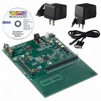
KIT DEV FOR ADUC832 QUICK START
Manufacturer
Analog Devices Inc
Series
QuickStart™ Kitr
Type
MCUr
Specifications of EVAL-ADUC832QSZ
Contents
Evaluation Board, Cable, Power Supply, Software and Documentation
Lead Free Status / RoHS Status
Lead free / RoHS Compliant
For Use With/related Products
ADuC832
Lead Free Status / RoHS Status
Compliant, Lead free / RoHS Compliant
Other names
EVAL-ADUC832QS
EVAL-ADUC832QS
EVAL-ADUC832QS


ADuC832
TABLE OF CONTENTS
Features .............................................................................................. 1
Applications ....................................................................................... 1
Functional Block Diagram .............................................................. 1
General Description ......................................................................... 1
Revision History ............................................................................... 4
Specifications ..................................................................................... 6
Absolute Maximum Ratings .......................................................... 20
Pin Configuration and Function Descriptions ........................... 21
Typical Performance Characteristics ........................................... 26
Terminology .................................................................................... 29
Explanation of Typical Performance Plots .................................. 30
Memory Organization ................................................................... 31
Special Function Registers (SFRs) ................................................ 33
Special Function Registers ............................................................. 34
ADC Circuit Information .............................................................. 35
Calibrating the ADC ...................................................................... 43
Timing Specifications ................................................................ 10
ESD Caution ................................................................................ 20
ADC Specifications .................................................................... 29
DAC Specifications..................................................................... 29
Flash/EE Program Memory ...................................................... 31
Flash/EE Data Memory ............................................................. 31
General-Purpose RAM .............................................................. 31
External Data Memory (External XRAM) .............................. 32
Internal XRAM ........................................................................... 32
Accumulator SFR (ACC) ........................................................... 33
B SFR (B) ..................................................................................... 33
Stack Pointer (SP and SPH)....................................................... 33
Data Pointer (DPTR) ................................................................. 33
Program Status Word (PSW) .................................................... 33
Power Control SFR (PCON) ..................................................... 33
General Overview ....................................................................... 35
ADC Transfer Function ............................................................. 35
Typical Operation ....................................................................... 35
Driving the Analog-to-Digital Converter ............................... 39
Voltage Reference Connections ................................................ 40
Configuring the ADC ................................................................ 41
ADC DMA Mode ....................................................................... 41
Micro-Operation During ADC DMA Mode .......................... 42
ADC Offset and Gain Calibration Coefficients ..................... 42
Rev. A | Page 2 of 92
Initiating Calibration in Code ...................................................... 44
Nonvolatile Flash/EE Memory ..................................................... 45
Using The Flash/EE Data Memory .............................................. 48
User Interface to Other On-Chip ADuC832 Peripherals ......... 51
On-Chip PLL................................................................................... 54
Pulse-Width Modulator (PWM) .................................................. 55
PWM Modes of Operation............................................................ 56
Serial Peripheral Interface ............................................................. 58
I
2
C-Compatible Interface .............................................................. 60
Flash/EE Memory Overview .................................................... 45
Flash/EE Memory and the ADuC832 ..................................... 45
ADuC832 Flash/EE Memory Reliability ................................. 45
Using the Flash/EE Program Memory .................................... 46
Flash/EE Program Memory Security ....................................... 47
ECON—Flash/EE Memory Control SFR ................................ 48
Example: Programming the Flash/EE Data Memory ............ 49
Flash/EE Memory Timing ........................................................ 49
ADuC832 Configuration SFR (CFG832) ................................ 50
DAC .............................................................................................. 51
Using the DAC ............................................................................ 52
PLLCON (PLL Control Register) ............................................. 54
PWMCON (PWM Control SFR) ............................................. 55
Mode 0: PWM Disabled ............................................................ 56
Mode 1: Single Variable Resolution PWM ............................. 56
Mode 2: Twin 8-Bit PWM ......................................................... 56
Mode 3: Twin 16-Bit PWM ....................................................... 56
Mode 4: Dual NRZ 16-Bit Σ-Δ DAC ....................................... 57
Mode 5: Dual 8-Bit PWM ......................................................... 57
Mode 6: Dual RZ 16-Bit Σ-Δ DAC .......................................... 57
MISO (Master Input, Slave Output Data Pin) ............................ 58
MOSI (Master Output, Slave Input Pin) ................................. 58
SCLOCK (Serial Clock I/O Pin) .............................................. 58
SS (Slave Select Input Pin)......................................................... 58
Using the SPI Interface .............................................................. 59
SPI Interface—Master Mode .................................................... 59
SPI Interface—Slave Mode ........................................................ 59
I
Overview ..................................................................................... 61
Software Master Mode ............................................................... 61
Hardware Slave Mode ................................................................ 61
2
C Interface SFRs ....................................................................... 60
Related parts for EVAL-ADUC832QSZ
Image
Part Number
Description
Manufacturer
Datasheet
Request
R


Part Number:
Description:
BOARD EVAL FOR SI270X-A
Manufacturer:
Silicon Laboratories Inc
Datasheet:

Part Number:
Description:
BUCK CONV REF DESIGN KIT IP1201
Manufacturer:
International Rectifier
Datasheet:
Part Number:
Description:
BOARD DEMO SYNC DUAL BUCK CNVTER
Manufacturer:
International Rectifier
Datasheet:
Part Number:
Description:
BOARD DEMO SYNC BUCK CONVETER
Manufacturer:
International Rectifier
Datasheet:

Part Number:
Description:
EVALBOARD/EB Omnidirectional microphone - Analog
Manufacturer:
Analog Devices
Datasheet:
Part Number:
Description:
EVALBOARD/EB Omnidirectional microphone - Analog
Manufacturer:
Analog Devices
Datasheet:


Part Number:
Description:
BOARD EVAL LED DRIVER LT3756
Manufacturer:
Linear Technology
Datasheet:

Part Number:
Description:
BOARD EVAL FOR AD7741/7742
Manufacturer:
Analog Devices Inc
Datasheet:

Part Number:
Description:
±1.7g Dual-Axis IMEMS Accelerometer Evaluation Board
Manufacturer:
Analog Devices Inc
Datasheet:

Part Number:
Description:
IC MULTIPLIER ANALOG 8-SOIC T/R
Manufacturer:
Analog Devices Inc
Datasheet:

Part Number:
Description:
IC ANALOG MULTIPLIER 8-DIP
Manufacturer:
Analog Devices Inc
Datasheet:
Part Number:
Description:
IC ANALOG MULTIPLIER 8-SOIC
Manufacturer:
Analog Devices Inc
Datasheet:
Part Number:
Description:
IC ANALOG MULTIPLIER 8-DIP
Manufacturer:
Analog Devices Inc
Datasheet: